
Resistor-Capacitor (RC) Snubber Design for Power Switches
über
Contributed By Digi-Key Corporation
2014-08-06
The power switches are the heart of every power converter. Their operation will directly determine the reliability and efficiency of the product. To enhance the performance of the switching circuit of power converters, snubbers are placed across the power switches to suppress voltage spikes and damp the ringing caused by circuit inductance when a switch opens. Proper design of the snubber can result in higher reliability, higher efficiency and lower EMI. Among many different kinds of snubbers, the resistor-capacitor (RC) snubber is the most popular snubber circuit. This article explains why a snubber is needed for power switches. Some practical tips for an optimum snubber design are provided as well.

There are many different topologies used in power converters, motor drivers and lamp ballasts. Figure 1 shows four basic power switching circuits. Within all of these four fundamental circuits, and in most power switching circuits, the same switch-diode-inductor network is shown within the blue lines. The behavior of this network is the same in all these circuits. Therefore, a simplified circuit as shown in Figure 2 can be used for the switching performance analysis for the power switches during a switching transient. Since the current in the inductor almost does not change during a switchifng transient, the inductor is replaced with a current source as shown in the figure. The ideal voltage and current-switching waveform of the circuit is also shown in Figure 2.

When the MOSFET switch turns off, the voltage across it rises. The current IL, however, will keep flowing through the MOSFET until the switch voltage reaches Vol. The current IL begins to fall once the diode turns on. When the MOSFET switch turns on, the situation is reversed as shown in the figure. This type of switching is referred to as “hard switching”. The maximum voltage and maximum current must be supported simultaneously during the switching transient. Therefore, this “hard switching” exposes the MOSFET switch to high stress.

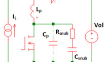
In practical circuits, the switching stress is much higher because of the parasitic inductance (Lp) and capacitance (Cp) as shown in Figure 4. Cpincludes the output capacitance of the switch and stray capacitance due to PCB layout and mounting. Lp includes the parasitic inductance of the PCB route and MOSFET lead inductance. These parasitic inductances and capacitances from the power devices form a filter that resonates right after the turn-off transient, and therefore superimposes excessive voltage ringing to the devices as shown in Figure 3. To suppress the peak voltage, a typical RC snubber is applied across the switch as shown in Figure 4. The value of the resistor must be close to the impedance of the parasitic resonance which it is intended to damp. The snubber capacitance must be larger than the resonant circuit capacitance, but must be small enough in order to keep the power dissipation of the resistor to a minimum.

Where power dissipation is not critical, there is a quick design approach for the RC snubber. Empirically, choose the snubber capacitor Csnubequal to twice the sum of the switch output capacitance and the estimated mounting capacitance. The snubber resistor Rsnub is selected so that
When this simple and empirical design does not limit the peak voltage sufficiently, then the optimizing procedure will be applied.
Optimized RC snubber: In those cases where power dissipation is critical, a more optimum design approach should be used. First, measure the ringing frequency (Fring) at the MOSFET switch node (SW) when it turns off. Solder a film type 100 pF low-ESR capacitor across the MOSFET. Increase the capacitance until the ringing frequency is half of the original measured value. Now the total output capacitance of the switch (the added capacitance plus original parasitical capacitance) is increased by a factor of four as the ringing frequency is inversely proportional to the square root of the circuit’s inductance capacitance product. So the parasitic capacitance Cp is one-third of the externally added capacitor value. The parasitic inductance Lp now can be obtained by using the following equation:

Once the parasitic inductance Lp and parasitic capacitance Cp are figured out, the snubber resistor Rsnub and capacitor Csnub can be chosen based on following calculation.

The snubber resistor can be fine-turned further to reduce the ringing if it is found to be insufficient.
The power dissipation on Rsnub at a given switching frequency (fs) is
Using all of the calculated values, the design for the power supply switch snubber is complete and can be implemented in the application.
Disclaimer: The opinions, beliefs, and viewpoints expressed by the various authors and/or forum participants on this website do not necessarily reflect the opinions, beliefs, and viewpoints of Digi-Key Corporation or official policies of Digi-Key Corporation.
Diskussion (0 Kommentare)