
Soft start for benchtop power supplies [160383]
Allows on/off switching of the output of a power supply without switching it off; also limits inrush current of the load.
By: Fons Janssen A benchtop power supply is an indispensable piece of equipment for the electronics lab. On most models, the only way to switch the output on and off is to hit its power switch. A switch or button to control the output only would be nice. A simple ON/OFF switch between the output of the power supply and its output terminals would do the trick, but bouncing of this switch and large inrush currents (if the load contains large capacitors) make this solution less attractive.
The circuit we present here solves these two issues by controlling the output voltage with constant dV/dt when the output power is switched on. A simple push button toggles the output.
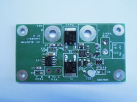
Figure 1 shows the schematic. The combination of FETs T1 and T2 is the ‘electronic switch’ that controls the output. The output of the benchtop power supply is connected to K1 (Vin), the load is connected to K2 (Vout). The MAX16126 (IC2) is a charge pump that increases the gate-source voltages of the FETs to approximately 9V, enough to open the FETs completely and minimize their Rdson. The voltage on K2 will follow the gate voltage minus the threshold voltage of the T1 and T2. Linear control of the gate voltage results in a linear rise of output voltage Vout to the level of the input voltage Vin. The charge pump acts like a current source (approx. 180 microamps) and C4 determines the slope:
I = C * dV/dt
This results in dV/dt = 180µA/220nF = 818V/s
If there’s a 1000µF capacitor connected to the output, the inrush current is limited to approximately 800V/s * 1000µF = 800mA, which is quite acceptable for most benchtop power supplies. You can change this value by tweaking C4.
IC3 (MAX16054) debounces on/off push button S1 and toggles a logic level that switches the charge pump on and off. Bicolor LED LED1 signals if the output is switched on or off. The inverted output of IC3 switches FET T3, which discharges the input capacitance of the load when switched off.
IC1 is a linear voltage regulator for the 5V supply of IC3 and IC2 when the output voltage of the benchtop power supply is lower than 5V. You can connect any internal constant DC voltage (up to 65V) of the benchtop to K3 to power this project. Alternatively, if your benchtop power supply does have an internal constant 5VDC, you can connect this directly to K4 and omit IC1.
D1 and D2 ensure that the input voltage of IC2 is not lower than 4.4V (minimum input voltage IC2 is 3V). If the output voltage of the power supply is less than 4.4V, the Vgs of T1 and T2 will be higher than 9V: 4.4V + 9V – Vin to be more precise. No issue for these FETs, which can sustain a maximum Vgs of 20VDC.
This circuit is designed for power supplies with a maximum output voltage of 30V. IC2 monitors the voltage with divider R6 and R7 and switches the FETs and the output off when Vin > 30V.
Assembling the PCB is quite a challenge, start with soldering IC2, preferably with a hot air soldering station (assuming that you don't have a reflow oven, which is of course even better). Use a magnifying glass or microscope to check the solder joint before you proceed with the rest of the PCB, which will be a piece of cake once you have a perfectly soldered IC2. Resistors and capacitors in 0805 case can also be replaced by 0603 ones.
The schematic of your benchtop power supply may be handy when you install this circuit. Please note that opening the case will void warranty -if still applicable- and of course unplug the mains voltage!
Since this is a universal solution, there is nog standard procedure or recipe for connecting this soft-start circuit.
BOM
Resistor
R1 = 100 Ω, thick film, 5%, 0.1W, 150V
R2,R7 = 10 kΩ, thick film, 5%, 0.1W, 150V
R3,R4 = 1 kΩ, thick film, 5%, 0.1W, 150V
R5 = 3.6k, 150V, 125mW, 1%, 0805
R6 = 240k, 150V, 125mW, 1%, 0805
Inductor
Capacitor
C1 = 100 nF, 50 V, X7R, 0805
C2 = 22µF, 10V, X5R, 20%, 1206
C3 = 1µF, 50V, 10%, X7R, 1206
C4 = 220 nF, 50 V, X7R, 0805
C5 = 1nF, 50V, 10%, X7R, 0603
Semiconductor
D1,D2 = 1N4148WS, 100 V, 200 mA, 4 ns
LED1 = bi Color LED red/green 3mm
T1,T2 = n-channel MOSFET 100V 41A NVD6824NLT4G
T3 = 2N7002, 60 V, 250 mA, 300 mW, Vgs=4.5 V, Rdson=1 Ω
IC1 = regulator 5V/150mA LDO MAX5024
IC2 = Voltage supervisor MAX16126TCA+
IC3 = Push button debouncer MAX16054AZT+T
Other
K1 = Terminal block 5.08 mm, 2-way, 630 V
K2A = see text
K2B = Terminal block 5.08 mm, 2-way, 630 V
K3,K4 = Pin header, breakable, 1 row, 2-way, vertical
S1 = push button NO (e.g. Multicomp R13-24A-05-BR)
Misc.
PCB 160383-1 V1.1
The circuit we present here solves these two issues by controlling the output voltage with constant dV/dt when the output power is switched on. A simple push button toggles the output.
Figure 1 shows the schematic. The combination of FETs T1 and T2 is the ‘electronic switch’ that controls the output. The output of the benchtop power supply is connected to K1 (Vin), the load is connected to K2 (Vout). The MAX16126 (IC2) is a charge pump that increases the gate-source voltages of the FETs to approximately 9V, enough to open the FETs completely and minimize their Rdson. The voltage on K2 will follow the gate voltage minus the threshold voltage of the T1 and T2. Linear control of the gate voltage results in a linear rise of output voltage Vout to the level of the input voltage Vin. The charge pump acts like a current source (approx. 180 microamps) and C4 determines the slope:
I = C * dV/dt
This results in dV/dt = 180µA/220nF = 818V/s
If there’s a 1000µF capacitor connected to the output, the inrush current is limited to approximately 800V/s * 1000µF = 800mA, which is quite acceptable for most benchtop power supplies. You can change this value by tweaking C4.
IC3 (MAX16054) debounces on/off push button S1 and toggles a logic level that switches the charge pump on and off. Bicolor LED LED1 signals if the output is switched on or off. The inverted output of IC3 switches FET T3, which discharges the input capacitance of the load when switched off.
IC1 is a linear voltage regulator for the 5V supply of IC3 and IC2 when the output voltage of the benchtop power supply is lower than 5V. You can connect any internal constant DC voltage (up to 65V) of the benchtop to K3 to power this project. Alternatively, if your benchtop power supply does have an internal constant 5VDC, you can connect this directly to K4 and omit IC1.
D1 and D2 ensure that the input voltage of IC2 is not lower than 4.4V (minimum input voltage IC2 is 3V). If the output voltage of the power supply is less than 4.4V, the Vgs of T1 and T2 will be higher than 9V: 4.4V + 9V – Vin to be more precise. No issue for these FETs, which can sustain a maximum Vgs of 20VDC.
This circuit is designed for power supplies with a maximum output voltage of 30V. IC2 monitors the voltage with divider R6 and R7 and switches the FETs and the output off when Vin > 30V.
Assembling the PCB is quite a challenge, start with soldering IC2, preferably with a hot air soldering station (assuming that you don't have a reflow oven, which is of course even better). Use a magnifying glass or microscope to check the solder joint before you proceed with the rest of the PCB, which will be a piece of cake once you have a perfectly soldered IC2. Resistors and capacitors in 0805 case can also be replaced by 0603 ones.
The schematic of your benchtop power supply may be handy when you install this circuit. Please note that opening the case will void warranty -if still applicable- and of course unplug the mains voltage!
Since this is a universal solution, there is nog standard procedure or recipe for connecting this soft-start circuit.
BOM
Resistor
R1 = 100 Ω, thick film, 5%, 0.1W, 150V
R2,R7 = 10 kΩ, thick film, 5%, 0.1W, 150V
R3,R4 = 1 kΩ, thick film, 5%, 0.1W, 150V
R5 = 3.6k, 150V, 125mW, 1%, 0805
R6 = 240k, 150V, 125mW, 1%, 0805
Inductor
Capacitor
C1 = 100 nF, 50 V, X7R, 0805
C2 = 22µF, 10V, X5R, 20%, 1206
C3 = 1µF, 50V, 10%, X7R, 1206
C4 = 220 nF, 50 V, X7R, 0805
C5 = 1nF, 50V, 10%, X7R, 0603
Semiconductor
D1,D2 = 1N4148WS, 100 V, 200 mA, 4 ns
LED1 = bi Color LED red/green 3mm
T1,T2 = n-channel MOSFET 100V 41A NVD6824NLT4G
T3 = 2N7002, 60 V, 250 mA, 300 mW, Vgs=4.5 V, Rdson=1 Ω
IC1 = regulator 5V/150mA LDO MAX5024
IC2 = Voltage supervisor MAX16126TCA+
IC3 = Push button debouncer MAX16054AZT+T
Other
K1 = Terminal block 5.08 mm, 2-way, 630 V
K2A = see text
K2B = Terminal block 5.08 mm, 2-way, 630 V
K3,K4 = Pin header, breakable, 1 row, 2-way, vertical
S1 = push button NO (e.g. Multicomp R13-24A-05-BR)
Misc.
PCB 160383-1 V1.1
Diskussion (0 Kommentare)