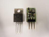
After having designed a switched [nodepicker==node/1952==Switched%207805%20Replacement==7805%20replacement] it was suggested that I should make a matching negative variant, a switched 7905 replacement. I knew that converting a positive DC voltage to a negative DC was possible, but I had never heard of a switched negative to negative DC convertor. So after a bit of research I found a topology called "Negative Buck Convertor" in an old National Semiconductor application note. It abuses an asynchronous boost convertor to convert a low negative DC voltage to a higher negative DC voltage. Just like an 7905. And I did manage to keep the PCB dimensions in check, as can be seen in the photo.
It is all a bit experimental, so what the final specs will be is still unknown. But I aim for an input is low as -18V which can still output 0,8A at -5V.
Update:
I assembled it and tested it with a light load and it works!!! -12V in, -5V out.
I've still got some tests to do. I will keep you posted.
Update1:
I did some tests with different input voltages, -17V till -8V works but higher than that gives incorrect output voltages.
Update2:
I am pretty sure the problem is the value of resistor R3. The simplified formulla states that Vout = Vref*(R1/R2). R3 is usually not a factor but I think it does become a factor when the input voltage approaches Vout. I've got to check my calculations again...
Update3:
I can't seem to get it right, R3 is only optimal for a certain -Vin. So I'm going to redesign the feedback with a current shunt monitor. So it's a resistor divider from GND to R1 to R2 to -Vout. After a bit of math the new output voltage could be calculated by this formula if you monitor over R1:
|Vout| = Vref / A*(R1/R2)
I'll draw up a new schematic.
Update4:
I chose a MAX4073T as a current shunt amp. Mainly because of the response time and small signal bandwith. It's input bias current is a bit high though, so I do have to waste a few mA in the feedback. This does hurt the efficiency but I think it's the right tradeoff. I modified the PCB so I've got to order some new ones... I'll keep you posted!
Update5:
Succes! Using that current sense amplifier was the right choice. I drop out at -5,5V with a -5V output. efficiency ranges from 87% down to 71% depending on input voltage. There are no startup issues at the moment. I'm going to put my test results in an excel sheet, try some diffrent loads and finally I plan to do a pulsed load test.
Update6:
I put my test results in an excel sheet, see the .zip on this page. I tested an approximate load of 60mA and a 560mA load. I also did those tests with an 7905(cooled!) for comparison, I was forced to ad a 47uF capasitor on the input and output to keep it stable, I didn't retest my replacement in this new, 'capacitance rich' setup. I also added some graphs to compare the two.
And I did a load step test, on my design. I added the scope shots. Its a 50KHz load step going from 60mA to 560mA and back. I am pleased to see that the internal compensation circuits still function well in this setup. The test setup did have those extra 47uF capacitors attached.
Update7:
I wanted to see an overload situation so I attached a 6 Ohm load resulting in a 833mA current if the output voltage remains a nice and clean -5V. The results are added to the excel file downloadable on this page. You can clearly see the switch current limit resulting in a less negative voltage. As you perhaps know, when the input output voltage differential increases, the duty cycle of the switch lowers, but the current will have to increase to transfer the required power to the load.
It was nice to see the limits of my design. I compared it to the 7905(cooled!), see excel file, it handles these higher loads better, but still at worse efficiencies.
Also something you don't see in my test results is when my prototype runs into it's switch's current limit the output voltage becomes very thermally dependant, simply blowing on it caused the output voltage too become more negative. So either the switch current limit is thermally dependant or the feedback circuit drifts with temperature fluctuations or the current is limited for thermal reasons. But somhow that last one seems less likely.

Diskussion (0 Kommentare)