
Spectrum Analyzer
32 kHz bandwidth 24 bits ADC , so noise floor at about 120 dB Interfacing with PC Single channel White noise generator Can make Bode plot
I intend to make a spectrum analyzer to analyze low distortion audio systems. I want to use a 24 bit ADC at 64 kHz.It will operate at a clock of 1024 kHz, so with an oversampling rate of 16 times.
When the ADC has taken a sample (15.625 us between samples) there are about 15 us available to read the data in serial format. The data can be clocked out by the SCLK- signal (Serial Clock) of at least 1.6 MHz. This can be done by at 64 MHz uP. A 24 bit shift register will be used to catche the sample. When 64 k samples are taken, the data will be transported to the PC. There the FFT wil be executed and the gathered data can be displayed.
Intended specifications:
Sampling rate 64 KHz
Noise floor about -120dB
Maximum input 5 V or 50 V peak. (internal attanuator)
Horizontal resolution 1, 2 or 4 Hz. (selectable)
Time for displaying one sample with high resolution:
taking sample: 1 s.
Transport: 12 s.
Making FFT:
Power dissipation: Expected < 2 W
Costs: Components < € 50
PCB € 100
Case < € 20
Needed time to complete project: 1 year
2025-10-17
Added: first circuit diagrams, preliminary.
2025-10-22
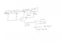
Some elucidation at the circuit diagram.The used ADC is the AD7767-1. The signal is coming in at X101 at the left of the "Front End". There are two attenuation stages for 5x and 2x attenuation (14 and 6 dB). The input circuit can handle + / - 5 V. The maximum input at X101 is + / - 50 V, 35 Vrms. When the input is too high the output of IC103 comes out of the range of Vref and will switch off the reed relais for maximum attenuation.
On the page "Digital" we see the uP PIC18F44K22. The memory is not important but I need a lot of outputs to control the ADC and the memory. At he low side of the page there is the shift register with IC202, 205 and 208. They are accompanied by latches IC220, 206, 209. IC207 is a 2-Mbit memory. IC204 and 210 form an 18 bit adrescounter for the memory. The uP, latches and the memory share an 8-bit data bus. To prevent ground loops isolator IC212 is added. IC215 translates RS232 to an USB -signal.
I have added a "Noise Generator" in order to ease measurements at audio equipment. It consists of a 16-bit shift register, sot it generates a sequence of maximum 2^16 - 1. IC306, 307 and 310 detect when there all ones in the register and can trigger the start of the AD-conversion. This makes comparison of audio circuits possible and an BODE-plot can easily be calculated.
2025-11-18
When the ADC has taken a sample (15.625 us between samples) there are about 15 us available to read the data in serial format. The data can be clocked out by the SCLK- signal (Serial Clock) of at least 1.6 MHz. This can be done by at 64 MHz uP. A 24 bit shift register will be used to catche the sample. When 64 k samples are taken, the data will be transported to the PC. There the FFT wil be executed and the gathered data can be displayed.
Intended specifications:
Sampling rate 64 KHz
Noise floor about -120dB
Maximum input 5 V or 50 V peak. (internal attanuator)
Horizontal resolution 1, 2 or 4 Hz. (selectable)
Time for displaying one sample with high resolution:
taking sample: 1 s.
Transport: 12 s.
Making FFT:
Power dissipation: Expected < 2 W
Costs: Components < € 50
PCB € 100
Case < € 20
Needed time to complete project: 1 year
2025-10-17
Added: first circuit diagrams, preliminary.
2025-10-22
Some elucidation at the circuit diagram.The used ADC is the AD7767-1. The signal is coming in at X101 at the left of the "Front End". There are two attenuation stages for 5x and 2x attenuation (14 and 6 dB). The input circuit can handle + / - 5 V. The maximum input at X101 is + / - 50 V, 35 Vrms. When the input is too high the output of IC103 comes out of the range of Vref and will switch off the reed relais for maximum attenuation.
On the page "Digital" we see the uP PIC18F44K22. The memory is not important but I need a lot of outputs to control the ADC and the memory. At he low side of the page there is the shift register with IC202, 205 and 208. They are accompanied by latches IC220, 206, 209. IC207 is a 2-Mbit memory. IC204 and 210 form an 18 bit adrescounter for the memory. The uP, latches and the memory share an 8-bit data bus. To prevent ground loops isolator IC212 is added. IC215 translates RS232 to an USB -signal.
I have added a "Noise Generator" in order to ease measurements at audio equipment. It consists of a 16-bit shift register, sot it generates a sequence of maximum 2^16 - 1. IC306, 307 and 310 detect when there all ones in the register and can trigger the start of the AD-conversion. This makes comparison of audio circuits possible and an BODE-plot can easily be calculated.
2025-11-18
The planned 74HC594 are replaced by 74HC595 for the shift tegister. They have a latch and a tristate output, this eliminates the need for the 74HC573.
Counters 74HC112 are replaced by 74HC73.
2026 -04-10
The first sample is up and operating. See the added circuit diagram and the premininary result. Still a lot of software work has to be done. Will be continued.
2025-05-17
2026 -04-10
The first sample is up and operating. See the added circuit diagram and the premininary result. Still a lot of software work has to be done. Will be continued.
2025-05-17
The power use is very low, making it possible to use USB bus power. However the CY7C65213 is configured to draw max 100 mA from the USB bus. For using bus power for the Spectrum Analyzer, we need about 250 mA. Older computer do not bother about this, but newer computers follow the standard. We can increase the max current to 500 mA by following the next steps:
- Go to MyInfineon.com on the internet. Register yourself, then log in.
- Once logged in, go to the tab Design Resources.
- Then go to the subtab Tools.
- You get a list, from this list select Configuration.
- You get another list. From this list select USB Uart Config Utility
- Then download USB Conguration Utility.
- Once downloaded and unpacked, close MyInfineon.com and find the map Cypress on your computer. In my case it was in the map ProgramFiles (x86).
- Open the map and go to the map USB-serial SDK.
- In the map documentation you find the manual for the Cypress USB Serial Configuration Utility. I suggest to take note of this, so you have any idea of what you are doing.
- Go to the map: bin and find the USB Serial Configuration Utility.exe
- In this stage you should have your Spectrum Analyzer connected via USB.
- Follow the manual. You can change the max current. Change this to 500 mA. In the same session change the maximum Baud rate from 115200 to 230400. Hopefully we can use it later.
- If you are done, press Program.
- Ready.
2026-05-19
On the photographs you see a few components which do not fit in the lay-out. In the latest files they are in the lay-out.
2026-05-22
In the partslist is one part which has a limited avalability. It concerns X-tal oscillator XO101.
At this moment it is stil availeable at Farnell with order code 3264069. At he moment of writing there are 592 pieces availeable.
2026-06-02
The large signals at the input caused a linearity issue. To solve this, I changed the Vref from 5 V to 2.5 V. Component D101 has to change to LM4040DYM3-2.5, OC: 2509865, price €0.32.
The problem seems to be solved, but the maximum input voltage is now limited to 50 Vpp, 17.5 Vrms.
2026-06-08
On assembling
Start with th IC's, especially the ADC. This is vulnerable, as well electrically as mechanically. Do not wriggle the legs! If you have one, use a microscope. Do not close the solder joints yet.
Supply. Do not mount the rectifier. I used the DC/DC converter IH0512D together with two resistors in series with the supply lines. In the + 12 V line 39 Ω and in the - 12 V line 180 Ω. The resistors will also limit the RF noise which comes from the DC converter. The resistors are connected to C216 (+) and C217 (-) respectively. The input voltage connections are connected to 5VUSB and AGND.
Programming the uP. You can use the PICKIT3, 4 or 5 with the software of Mikrochip (MPlab).
The power supply has to be operating, so there has to be an USB connection. After programming you can close solder-joints PGD and PGC on top of the board. Also close SJ1 and SJ301 at the bottom. If reprogramming is necessary, first open PGC and PGD.
The board shall now be operational.
Housing and shielding. This analyzer is very sensitive, it can measure below 1 μV. To prevent noise coming in a metal housing is the best. But also plastic with additional copper foil is OK. See the photographs how I did it. The copper foil and metal parts of the housing have to be grounded.
Use of the PC program.
At the moment of writing, the program is not finished, but good enough to play with. The first step will be alignment of the instrument. The 2.5 V source is chosen for its stability, but by use of a few resistors in the input stage the accuracy can be improved. The deviation can easily be a few percent.
Connect a stable voltage of about 2 V to the input. Measure the voltage with a trustworthy voltmeter. On the main screen go to Utilities and then to Alignment. Align potmeter R110 so that the readings on the screen and the voltmeter are equal.
2026-06-10
The PC program is written in basic. I used Justbasic, which is free to download. With this basic program it is possible to make a "tokenized" file, so the program can run without its editor. Unfortunately, a program made in this way runs slower than when it is ran in the editor. So it is not always a good idea to use it in this way. Depending on the speed of your computer it is better to use the program in the editor.
Diskussion (1 Kommentar)