
SCR gate pulse generator [180611-1]
This circuit generates mains synchronized gate pulses for thyristors, triacs and similar components or circuits for testing purposes.
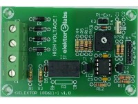
This circuit generates mains synchronized gate pulses for thyristors, triacs and similar components or circuits for testing purposes. Optocoupler CNY65 (IC1) is the zero crossing detector. Two standard 250 V 100 kΩ resistors (R1 and R2) are used to drive the led inside the optocoupler. When the voltage applied to K2 is considerably lower it can be necessary to lower the values of these resistors (when using LV circuit 160515-1). This optocoupler makes a clearance distance of more than 6 mm for safety between the layout of the high voltage (HV) side and low voltage (LV) side of the PCB possible. If needed both sides can be connected by a 0 Ω resistor or a jumper wire (R3). But be aware that the whole circuit is connected to the mains voltage then, especially connector K4!!! This connecting of the LV and HV side can be necessary when the output +HV from the full wave rectifier D1..D4 (K1) is used (needed by LV circuit 160515-1). The optocoupler signal is inverted, buffered and amplified by transistor T1 (BC547B) . IC2 is a dual comparator of type LM393. It has a common mode input from 0 V to 1.5 V (at 25°C) below the positive power supply rail. If one input is within this common mode range and the other one is above it there’s no phase reversal at the open collector output. Comparator IC2A and IC2B both have a 2.5V reference voltage generated by a voltage divider formed by resistors R11 and R12 and decoupled with C4. Potentiometer P1 and capacitor C1 set the pulse RC time constant. C2 is not used and reserved if the control needs to be more precise or needs to be adapted for 60 Hz. Potentiometers typically have a tolerance of 20 %. Then (C1+C2)*P1 is the RC time constant. Diode D6 discharges the capacitor C1 right after the zero crossing. The full wave rectifier +HV output frequency is 100 Hz (K1) when the mains frequency is 50 Hz (mains connected to K2). This output voltage from K1 can be used to power a SCR circuit containing a thyristor, triac or similar components. This circuit was originally designed for use with both ‘Two-anode MOSFET thyristor’ circuits (160515-1 v1.1 and 160515-1 v1.1) but it can be used for other applications as well. To make a more universal circuit connector K4 not only contains the pulse output signal but also the +5 V DC power supply voltage. An external +5 V power supply must be connected here. This means when 0 Ω resistor R3 is in place on the PCB this external +5 V power supply is also connected to the mains voltage when the mains voltage is connected to K2! Always be very careful when touching the circuit! Always remove the mains voltage when changing wiring etc. The 2.5 V reference voltage is also connected to K4, it can be either input or output. Depending on the application this can be useful. At K3 an external potentiometer can be connected, a plastic one! Remove the trimmer on the PCB otherwise they will be connected in parallel. Preferably use the trimmer and a The output stage around T2 is added to make sure the output voltage can really reach zero volt. Using a low-value resistor as a pull-up at the output of IC2B to drive the gate of a thyristor will still have some voltage at the output due to the open collector output of the comparator and can be the cause the thyristor is always triggered. The 330 Ω value for R9 will ensure most thyristors or triacs have enough gate current, more than 10 mA, to trigger properly. A typical use for this circuit can be found in project ‘Two-anode MOSFET thyristor’ where also a wiring diagram can be found.
At a first glance the single sided PCB (the pdf with topoverlay shows copper on the bottom side) is maybe a bit large but consider the safety rules implemented like 3 mm clearance where mains voltage is directly present. On the mains side of the PCB all traces have a 6 mm clearance to the edge of the PCB. DC isolation test voltage of a CNY65 is rated 13.9 kV (1 s.)! Component costs should be less than 10 euro.
Also see
https://www.elektormagazine.com/labs/two-anode-mosfet-thyristor-160515
Bill of materials
Resistor
R1,R2,R4 = 100 kΩ, 5%, 0.25W, 250 V
R3 = 0 Ω, 5%, 0.25W (or jumper wire)
R5,R6 = 1 kΩ, 5%, 0.25W
R7,R8 = 2.2 kΩ, 5 %, 0.25W
R9 = 330 Ω, 5%, 0.25W
R10,R11,R12 = 10 kΩ, 5%, 0.25W
P1 = 1 MΩ, trimmer, flat
Capacitor
C1 = 15 nF, 100 V, 10 %, PET, lead spacing 5/7.5 mm
C2 = leave open, see text
C3,C4 = 100 nF, 50 V, 10 %, X7R, lead spacing 5/7.5 mm
Semiconductor
D1-D4 = 1N4007, DO-41
D5,D6 = 1N4148, DO-35
T1 = BC547B, TO-92
T2 = BC557B, TO-92
IC1 = CNY65, DIP-4 HV (L x W = 17.8 x 9.6 mm)
IC2 = LM393P, DIP-8
Other
K1,K2 = Terminal block 7.68 mm, 2-way, 630 V
K3 = Pin header, 1 row, 2-way, vertical, pitch 2.54 mm
K4 = Pin header, 1 row, 5-way, vertical, pitch 2.54 mm
Optional socket for IC2 = 8 Contacts, DIP, 2.54 mm, 7.62 mm
Misc.
PCB 180611-1 v1.0
Diskussion (1 Kommentar)