
Custom power bank
Light and small power bank which can use all kind of standard old mobile battery, charging 4.2v to 4.4v and no sleep mode possible. Use of a specific IC IP5305T from Injoinic.
For some time, I was looking for some small power bank, getting tired with all current models which are heavy and bulky. Often, 2000mAh is enough to recover some hours of empty devices. Recently, my phone was out of battery and for a run, I did not want to take standard powerbank. I took this one, with the light Samsung 2000mAh battery. It was enough to power the phone (and had the music), charging little bit during 2h of run. Exactly what I needed.
Beside this, I have many old batteries, like for mobile phone, with different chemistry which request charging voltage from 4.2v, 4.3v, 4.35v or 4.4v.
There is some Chinese IC manufacturers, dedicated for power bank, with single inductor, for buck (charging) and boost (for delivery 5V) capability. One well known is Injoinic. In the list of all possible IC, Injoinic has one old model, IP5305T, which can charge up to 1.2A, deliver 5v 1A, and more important, can select the end voltage charging with an Rset simple resistor. Last, the packaging is SO8 which is easy to use for us. Maybe there are some other options (SO package, multiple charging voltage, low number of components) but I did not find.
Like many, if not all, power bank, there is a sleep mode feature which turn off the 5V output if the load current is lower than a fix value during a fix time. These values depend of the IC used and not clearly defined in the datasheet. To bypass this feature, in case of need some load low current, another module is added based on the IC 555 in astable mode but with pulse function (PWM).
Detail of the Buck-boost module:
The datasheet of IP5305T exists in Chinese (for the T version) and in english (for non T version). T version is mandatory for the ability to choose the end charging voltage.
There are several configuration possible for display charge or discharge level on 1, 2, 3 or 4 leds. Here, I use the 2 leds version. One led for charging (blinking during charging, fix at end of charging) and one for discharging (fix when battery ok, blinking when battery is low).
For selecting the end of voltage charging, a Rset resistor need to be add. No Resistor is 4.2V, 43k (4.3v), 75k (4.35v), 100k (4.4v), all 1% resistor. On this mockup, I use jumper for select end voltage. No need to say that this choice must be exactly link to the battery used. It can be dangerous to charge at higher voltage than the specification of the battery.
Some ceramic high capacitors are needed. It is important (and I made the mistake), to put some of them (Vbat, Vin, Vout) as close as possible of the IC, even for the mock up.
The inductor is recommended to be a CD43, 2.2uH (ISat around 2A). Good connection between inductor and the IC is needed.
One push button is used for power on (short press) or power off (2 short press). Long press is the a light function which is not used here.
An important point is the ground. There is no pin for the ground on this IC (I missed this point on the schematic). Need to use the body, under the SOP (kind of copper plane) to make the ground connection. On this mockup, I soldered a golden pin from an old connector under the IC before put it on the board and solder the regular pin.
The battery is connected via a JST 2.54mm connector.
Control section of the IP5305T:
There are some features called control center.
First, when we connect a device on the output, it's start automatically the Boost mode. The minimum current is around 50mA.
Then, if the boost mode is on, and no more load, the IC sleep and stop the boost mode after a certain time. In the spec, it is mentioned between 25 to 40 sec. On my sample, it is 40 seconds. Now, this is specific of the IC used and some other brands can be at 5 sec or higher than 40.
Also, and this is sometimes a problem, if the loading current decrease below a value, the boost mode is going to sleep and turn off the IC. In the specification, they mention 45mA but the tests I've done showed that it is more around 120mA (39 ohm).
Module to avoid sleep mode:
As I often use power bank to recharge other batteries devices, big or small, to have a shut down of the output below 130mA is a serious inconvenient. There is no way to deactivate this feature. So, I'm using another way, which is to periodically, drain some current during brief time.
Some proposal of such feature was presented during a previous Summer Elektor magazine.
Here, I'll use a simple way with the famous NE555, 3 parameters need to be tune for this function:
- Total period (time between pulse): As the spec is 25-40 sec, 20 sec period is chosen
- Current to drain: 39 ohm which is 128mA under 5v
- Pulse time: There is no indication for that in the datasheet. I tried 1ms, 10ms, 100ms and finally, 320ms (or more) which is the only working one.
So, the NE555 is setup as astable, 20 sec period (R=470k+100k, C=47uF : (R*C)/1.44 = 18 sec.
The pulse is setup at 326ms (R = 10k C = 47uF : 326ms)
The difference between charging and discharging is made by using 2 diodes in opposite direction.
The output of the NE555, negative pulse, drives a PNP (2907) to the charge 39 ohm. An LED is put in parallel of the 39 ohm to visualize the pulse.
This module is put on an independent module through USB-A male and female, so, I can use it on other existing power bank.
A rough calculation to estimate the "over consumption" of this module is around 2mAh which, I think, can be accepted (326ms every 20 sec = around 1 sec / min so, 1 min for 1h. 128mA / 60 = 2mAh)
Conclusion:
Funny small project. I can carry now small power bank and several old smartphone batteries with different charging voltage.
The module to avoid sleep mode is very convenient but need to be adapt sometimes to other power bank specificities.
PCB and schematic are done now. In the documents. Waiting the PCB to test.
UPDATE JUNE 19th, 2025:
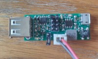
- Received PCB, assembled it and test. To solder the IP5305, I put first some solder past on the PCB under the IC and heat it with hot air gun at 400 degrees. After some second, it is soldered. Then I soldered the pins by hand.
All is ok. For some reason, the timing for the pulse to keep the IC on has to be adjusted (10k -> 22k => 640ms).
2 jumpers on the board. The first one is to select the end of charging voltage (from top to down 4.2v/4.3v/4.35v/4.4v). The second one to enable or not the function to keep the powerbank always ON.
Project finished. Some minor changes on the PCB has been done to facilitate the soldering.
Just plan to make small casing to fit all inside.
Laurent
Beside this, I have many old batteries, like for mobile phone, with different chemistry which request charging voltage from 4.2v, 4.3v, 4.35v or 4.4v.
There is some Chinese IC manufacturers, dedicated for power bank, with single inductor, for buck (charging) and boost (for delivery 5V) capability. One well known is Injoinic. In the list of all possible IC, Injoinic has one old model, IP5305T, which can charge up to 1.2A, deliver 5v 1A, and more important, can select the end voltage charging with an Rset simple resistor. Last, the packaging is SO8 which is easy to use for us. Maybe there are some other options (SO package, multiple charging voltage, low number of components) but I did not find.
Like many, if not all, power bank, there is a sleep mode feature which turn off the 5V output if the load current is lower than a fix value during a fix time. These values depend of the IC used and not clearly defined in the datasheet. To bypass this feature, in case of need some load low current, another module is added based on the IC 555 in astable mode but with pulse function (PWM).
Detail of the Buck-boost module:
The datasheet of IP5305T exists in Chinese (for the T version) and in english (for non T version). T version is mandatory for the ability to choose the end charging voltage.
There are several configuration possible for display charge or discharge level on 1, 2, 3 or 4 leds. Here, I use the 2 leds version. One led for charging (blinking during charging, fix at end of charging) and one for discharging (fix when battery ok, blinking when battery is low).
For selecting the end of voltage charging, a Rset resistor need to be add. No Resistor is 4.2V, 43k (4.3v), 75k (4.35v), 100k (4.4v), all 1% resistor. On this mockup, I use jumper for select end voltage. No need to say that this choice must be exactly link to the battery used. It can be dangerous to charge at higher voltage than the specification of the battery.
Some ceramic high capacitors are needed. It is important (and I made the mistake), to put some of them (Vbat, Vin, Vout) as close as possible of the IC, even for the mock up.
The inductor is recommended to be a CD43, 2.2uH (ISat around 2A). Good connection between inductor and the IC is needed.
One push button is used for power on (short press) or power off (2 short press). Long press is the a light function which is not used here.
An important point is the ground. There is no pin for the ground on this IC (I missed this point on the schematic). Need to use the body, under the SOP (kind of copper plane) to make the ground connection. On this mockup, I soldered a golden pin from an old connector under the IC before put it on the board and solder the regular pin.
The battery is connected via a JST 2.54mm connector.
Control section of the IP5305T:
There are some features called control center.
First, when we connect a device on the output, it's start automatically the Boost mode. The minimum current is around 50mA.
Then, if the boost mode is on, and no more load, the IC sleep and stop the boost mode after a certain time. In the spec, it is mentioned between 25 to 40 sec. On my sample, it is 40 seconds. Now, this is specific of the IC used and some other brands can be at 5 sec or higher than 40.
Also, and this is sometimes a problem, if the loading current decrease below a value, the boost mode is going to sleep and turn off the IC. In the specification, they mention 45mA but the tests I've done showed that it is more around 120mA (39 ohm).
Module to avoid sleep mode:
As I often use power bank to recharge other batteries devices, big or small, to have a shut down of the output below 130mA is a serious inconvenient. There is no way to deactivate this feature. So, I'm using another way, which is to periodically, drain some current during brief time.
Some proposal of such feature was presented during a previous Summer Elektor magazine.
Here, I'll use a simple way with the famous NE555, 3 parameters need to be tune for this function:
- Total period (time between pulse): As the spec is 25-40 sec, 20 sec period is chosen
- Current to drain: 39 ohm which is 128mA under 5v
- Pulse time: There is no indication for that in the datasheet. I tried 1ms, 10ms, 100ms and finally, 320ms (or more) which is the only working one.
So, the NE555 is setup as astable, 20 sec period (R=470k+100k, C=47uF : (R*C)/1.44 = 18 sec.
The pulse is setup at 326ms (R = 10k C = 47uF : 326ms)
The difference between charging and discharging is made by using 2 diodes in opposite direction.
The output of the NE555, negative pulse, drives a PNP (2907) to the charge 39 ohm. An LED is put in parallel of the 39 ohm to visualize the pulse.
This module is put on an independent module through USB-A male and female, so, I can use it on other existing power bank.
A rough calculation to estimate the "over consumption" of this module is around 2mAh which, I think, can be accepted (326ms every 20 sec = around 1 sec / min so, 1 min for 1h. 128mA / 60 = 2mAh)
Conclusion:
Funny small project. I can carry now small power bank and several old smartphone batteries with different charging voltage.
The module to avoid sleep mode is very convenient but need to be adapt sometimes to other power bank specificities.
PCB and schematic are done now. In the documents. Waiting the PCB to test.
UPDATE JUNE 19th, 2025:
- Received PCB, assembled it and test. To solder the IP5305, I put first some solder past on the PCB under the IC and heat it with hot air gun at 400 degrees. After some second, it is soldered. Then I soldered the pins by hand.
All is ok. For some reason, the timing for the pulse to keep the IC on has to be adjusted (10k -> 22k => 640ms).
2 jumpers on the board. The first one is to select the end of charging voltage (from top to down 4.2v/4.3v/4.35v/4.4v). The second one to enable or not the function to keep the powerbank always ON.
Project finished. Some minor changes on the PCB has been done to facilitate the soldering.
Just plan to make small casing to fit all inside.
Laurent
Build This Project
Bring this design to life with the Elektor PCB Service, powered by Eurocircuits. Upload the project files and order professionally manufactured PCBs or assembled boards through a proven European production platform.
Supporting KiCad, Eagle, Gerber, and ODB++ formats, the service is suitable for everything from prototypes and validation builds to series production and volume manufacturing.
Made in Europe. Fast. Reliable. Professional.
Diskussion (2 Kommentare)