
140169-2 Filter for Practical 4-channel ADC
A while back we made a little break-out-board with a ADS1115 A/D converter (140169-1). It has four inputs that can be used in a single-ended mode or two inputs can be used in a differential mode. A project still in development is a power meter for mains powered appliances.
A while back we made a little break-out-board with a ADS1115 A/D converter (140169-1). It has four inputs that can be used in a single-ended mode or two inputs can be used in a differential mode. A project still in development is a power meter for mains powered appliances. It is meant as a nice application for the A/D module, although its maximum bandwidth is maybe a bit small (maximum selectable sample frequency is 860 Hz).
To make the power meter safe we used differential isolation amplifiers (> 4 kV) with a switched-capacitor circuit at their input and a small-signal bandwidth of 100 kHz (typical). Of course this bandwidth is too large for the A/D module. To filter out the wide band noise and residual switching artifacts of the isolation amplifiers, we designed a little PCB with four third-order Butterworth filters in a standard Sallen-Key topology. In theory no frequencies beyond half the sample frequency should be present at the inputs of the A/D module. With a third order filter and 16 bit resolution the cut-off frequency would have to be around 10 Hz or so, not very practical for our power meter. Due to tolerances of especially the capacitors (resistors not so much) the bandwidth has to be considerably larger to prevent a phase variation between the filter outputs from degrading the differential signal from the isolation amplifiers. Taking into account that frequency components are maybe 30 dB below the fundamental frequency level. Bandwidth can then be 40 Hz or so, which is still too low. For the power meter we are primarily interested in the accurate amplitudes and phase of the mains voltage and current. The assumption is that the harmonics in modern equipment are not that great an influence on the power measurement. The component values for the filters (R1..R12, C1..C12) are calculated for a cut-off frequency of 1 kHz. That seems high but most of the noise will be filtered out. Also any phase variation at 50 or 60 Hz will be small.
We selected a rail-to-rail opamp from Texas Instrument, the OPA377. Availability and PCB layout were the reasons to use a single amplifier for each channel. Our aim is to measure very small signals. Consider a current of just 1 mA at 230 V, it’s almost a quarter of a Watt. Would be nice if we can measure 0.1 mA or less. The OPA377 is certainly not the cheapest one but it has an excellent noise performance for a CMOS input opamp. To keep the tolerance of the ceramic 0603 capacitors within 5 %, the highest value available was 22 nF. For resistors this means a fairly high value around 23 kΩ. Lower resistor values would improve noise performance but a low tolerance of the capacitors is more important because of potential phase difference between the individual filters. Input bias current of the OP377 is 0.2 pA typical (10 pA max.). So no extra offset is introduced by the resistors. Input offset and offset drift versus temperature are 1 mV max. (0.25 mV typical) and 0.32 µV/°C respectively. Any fixed DC offset can be compensated in software. Only very low frequency noise is relatively high, but this is typical for CMOS inputs.
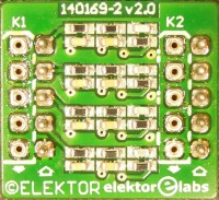
The PCB is designed to fit as an add-on between the ADC-PCB and the power meter (or any other application). To have it fit we tried to make it the same size as the ADC PCB (19.05 x 19.68 mm) but it’s 1/10” longer (21.59 x 19.68 mm). So if the components on the main PCB are not too close to the ADC PCB the filter should fit between them. To keep it that small both sides have components mounted. On top are the filter components R1..R12 and C1..C12. On the bottom side are the four OPA377s and their respective power supply decoupling capacitors (C13..C16). Input and output connector on the filter PCB are placed next to each other as close as possible (K1/K3). The same is true for K2 and K4. The power supply is taken from here (K4 is connected to the main board). These two connectors are simply connected in parallel. K1 and K2 are the connection to the ADC PCB and two 5way sockets can be used. We made holes for the pins big enough (1 mm holes) to also fit pcb sockets (also called discrete socket, discrete receptacle, etc.). One usable type is 2-5330808-7 from TE Connectivity/Amp. But even at 1000 pieces they are pretty expensive. So using normal sockets here is probably a more sensible way of connecting the two PCBs. Downside is the increase in height (distance between the two PCBs). On the bottom side two headers (male) with rounded pins are used for K3 and K4. The larger diameter is to be soldered into the PCB. The smaller ones will fit in the sockets on the main PCB.
Table 1 gives alternate E12 values for C1..C12 and their corresponding theoretical values for R1..R12. Cut-off frequency is always the same at exactly 1 kHz. For different frequencies it’s easy to recalculate the theoretical values of the resistors inverse proportionally and round them to the nearest E96 values. E24 and E12 will influence the pass band amplitude too much if it’s considered critical.
Table 1 (fc = 1 kHz)
C1 C2 C3 R1[kΩ] R2[kΩ] R3[kΩ]
10n 22n 1n5 21.452 24.424 23.316
8n2 18n 1n2 26.360 29.324 29.446
6n8 15n 1n 31.764 35.378 35.171
5n6 12n 820p 38.436 43.551 43.706
4n7 10n 680p 45.914 51.689 53.151
3n9 8n2 560p 55.352 62.410 65.165
3n3 6n8 470p 65.355 74.233 78.788
2n7 5n6 390p 79.619 91.225 94.127
2n2 4n7 330p 97.019 112.96 107.81
1n8 3n9 270p 118.87 136.91 130.70
1n5 3n3 220p 144.06 160.34 160.28
1n2 2n7 180p 179.44 200.93 191.72
We did some measurements with our Audio Precision Analyzer and were a bit disappointed by the result of the THD+N measurements, although not really important for our power meter. We expected a higher THD+N because of the ceramic filter capacitors, well at least somewhat higher than the datasheet of the opamp specifies (typ. 0.00027 % at 1 kHz and 1 VRMS). Current consumption with all inputs at 2.5 V (5 V supply) is roughly 2.8 mA.
Plot A (Amplitude_1V_in_BW_100kHz.png) shows amplitude as a function of frequency at the output of one of the filters. A bandpass was used to really measure as far down as possible. Input signal is 1 VRMS. At about 50 kHz the output levels at around 97 dB due to noise. From 2 kHz to 20 kHz it’s 60 dB down, exactly what you expect when using a third order filter.
Plot B (4xAmplitude_1V_in.png) zooms in at the cut-off frequency of the four filters, with the same 1 VRMS signal applied. Deviation between the amplitudes at 400 Hz is about 0.1 dB. That’s not bad, considering two capacitors in our prototypes were 5 % and the other one 10 % (22 nF). At 50 or 60 Hz there’s almost no deviation.
Plot C (4xPhase_1V_in_2.png) shows the phase as a function of frequency between input and output of the filters. At 50 or 60 Hz there’s hardly a deviation. So using separate filters for a differential input will not degrade the common mode rejection (of the ADC).
Plot D and E (4xTHD+NvsLVL.png and 4xTHD+NvsLVL_2.png) show the THD+N as a function of output level. Up to 1.15 V the steady increase in distortion is caused by the ceramic capacitors. The extra increase between 1.15 and 1.2 V is caused however by the opamp. This is something not to be found in the datasheet. A telltale in the datasheet is maybe the fact that some specifications are made at 1 VRMS (like THD+N). To be sure we removed the three capacitors in one channel (with the biggest step).
Plot F (THD+NvsLVL_no_caps.png) shows THD+N as a function of output level with the capacitors removed. The distortion caused in the previous plots is clearly gone (lower trace). THD+N at 1 V is now less than 0.0007 % (thermal noise from 70 kΩ is about 0.0005 %, B=22 kHz ). Its clear (if you didn’t know already) that the ceramic dielectric is probably the worst to use in audio. Lucky for us this filter is meant for meter applications and related. We can only guess that at some point the input becomes more non-linear. CMRR in the datasheet of the OPA377 is specified within 1.3 V of the power supply rails. Also input offset increases if the input is within 1 V of the power supply rails.
Plot G (Amplitude_1V_in_BW_100kHz_sym_in_out.png) shows the amplitude as a function of frequency when 2 filters are used for a differential in and output. We measured with full bandwidth of the analyzer and with a bandpass at 1 V. With full bandwidth the amplitude levels a little under 90 dB. With a bandpass we can see that the noise floor has dropped compared to the single ended measurement (Plot A). At 100 kHz the level is about -112 dB! That’s a 15 dB improvement compared to Plot A.
Plot H (THD+NvsLVL_sym_in_out.png) show THD+N as a function of output level. Compared to the single ended measurements the THD+N is has also improved, depending on the level a few hundreds of a percent. For a correct comparison the level of the differential measurement is twice the level of single ended one. We measured with 50 and 60 Hz (upper trace, green).
Bill of materials
Resistor
R1,R4,R7,R10 = 21k5, 1 %, 0W1, SMD 0603
R2,R5,R8,R11 = 24k3, 1 %, 0W1, SMD 0603
R3,R6,R9,R12 = 23k2, 1 %, 0W1, SMD 0603
Capacitor
C1,C4,C7,C10 = 10 nF, 5 %, 50 V, C0G/NP0 or X7R, SMD 0603
C2,C5,C8,C11 = 22 nF, 5 %, 50 V, C0G/NP0 orX7R, SMD 0603
C3,C6,C9,C12 = 1n5, 5 %, 50 V, C0G/NP0 or X7R, SMD 0603
C13,C14,C15,C16 = 100 nF, 10 %, 50 V, X7R, SMD 0603
Semiconductor
IC1,IC2,IC3,IC4 = OPA377AIDBVT
Other
K1,K2 = receptacle, through hole (5way), pitch 2.54 mm
K3,K4 = header, through hole (5way) pitch 2.54 mm
Misc.
PCB 140169-2 v2.0
Diskussion (0 Kommentare)