
10 MHz DDS Function Generator [150210]
Design and text by Theodorou Gerasimos (Greece) A few years ago I needed a frequency generator for my laboratory. I had worked on some expensive models and initially I thought to buy one. But none of them was what I was really looking for.
Design and text by Theodorou Gerasimos (Greece)
A few years ago I needed a frequency generator for my laboratory. I had worked on some expensive models and initially I thought to buy one. But none of them was what I was really looking for. So I decided to make my own generator. After researching various techniques I decided to use the DDS based architecture. This would result in simplification of the analog part of the generator. Also I could immediately start working on the digital part of the generator, the microcontroller and the DDS chip.
As microcontroller I chose one from the ARM7 series of Analog Devices which I thought was incredibly elegant. Also, the same company had plenty of DDS chip, from which I picket the AD9834. What's more, the AD website contained all the knowledge I needed.
As microcontroller I chose one from the ARM7 series of Analog Devices which I thought was incredibly elegant. Also, the same company had plenty of DDS chip, from which I picket the AD9834. What's more, the AD website contained all the knowledge I needed.
The parts around the AD9834 are recommended by the manufacturer (from the datasheet). The programming is done by SPI. The frequency of the external oscillator is 75 MHz. This is the maximum frequency which can be accepted by the chip. The 75MHz clock produces the cleanest possible sine at high frequencies but on the other creates errors at low frequencies. For example, if we want 20Hz output frequency.
F=∆Phase x fMCLK/2^28
From the above equation, we should load the ΔPhase with the value 71.58. But this register cannot take fractional value. Therefore we will load the value 71 to the ΔPhase register. Then the output frequency will not be 20Hz but according to the above equation Fout = 19.84Hz.
The output of the AD9834 is filtered by an RC network and then is amplified. A high-order filter is not needed.
The output signal from the AD9834 follows two paths. One path is used when the output waveform of the generator is sinusoidal or triangular. The other path is used when the output waveform of the generator is square. In this case (square output waveform) the AD9834 produces a triangular waveform to drive two opamps that form a relatively fast comparator with proper amount of hysteresis. The reference voltage for comparison is given by DAC0 of the ADUC7024. The DAC0 output level regulates the Duty Cycle of the square waveform. The ADG779 provides very good isolation between the two inputs and the output.
The output of the ADG779 drives potentiometer P2 and is then amplified by the current feedback opamp AD811. This opamp is quite fast (2500V / ms slew rate) and it is has a high output current. The pk-pk output level is adjusted by potentiometer P2. This potentiometer has a very important role in the quality of the output signal, because the potentiometer is a low pass filter. Its cut-off frequency is directly related to the number of turns of the potentiometer and its resistance. If our desire is a clean as possible sine at high frequencies then we should choose a 10 turns potentiometer with 1 kΩ resistance or more. On the other hand if we want a sharp square waveform at high frequencies then we should choose a 5 turns potentiometer with 200Ω resistance or less.
Let us consider again the subject of filtering. Observe the signal path when the output is sine waveform. The AD8042 is a low pass filter. Also the switch ADG779, potentiometer P2 and the AD811 are low pass filters. Even the tracks of the PCB are low pass filters. Essentially i.e. from the output of AD9834 to the output of generator are many low pass filters. Also if a high order filter is to be added then a separate path for triangular waveform must be designed.
The two voltage references type ADR1581 drive the potentiometer P1 which in turn drives the high precision opamp OP1177. This circuit controls the dc offset of the output. When the output of the OP1177 is 1 V then the AD811 will be forced to add -7 V DC offset to its output. Similarly when the output of the OP1177 is -0.4 V then the AD811 will be forced to add +7 V DC offset to its output.
The constant output voltage of 1.25 V is also used as a reference voltage for the level shifter circuit. The purpose of this circuit is the level shifting of the output waveform voltage (+ 15volt, -15volt) within the input range of ADC0 (0volts, + 2.5volts) of the ADUC7024.
The +/-15 V power supply consists of a pair of LM317, LM337. Another LM317 is used to produce the 3.3V. The construction was implemented with the LM3xx series because it is cheap and widely available and it has very good features.
The software was written in C. The well known uVision from Keil has been used as development environment.
The code consists of six files. Three of them are header files. The main.c file gathers the generator operation code. The epson6610.c or philips6610.c, depending on LCD controller, being the driver of the display. The init.s file was written in assembly and makes the necessary initialization of microcontroller.
About the driver of the display should be mentioned that there is a lot of free code for experimentation on the internet. The display, as seen from the schematic, is not connected to a real SPI interface but with general GPIO pins. SPI simulation code becomes from WriteLcdCommand functions () and WriteLcdData (). The LCD driver consists of about 10 functions in total. The initialization is done by InitLcd (). Eventually the whole effort was to transform the display into a 16x8 small characters or 8x4 large characters display.
The biggest part of the code is collected in file main.c. Polling method instead of interrupt has been used to monitor buttons. Code simply enters to an endless loop after initialization until a button is pressed. Then the corresponding function to that button is run. Furthermore an attempt was made with various programming methods not to use floating-point arithmetic, and mathematical libraries of C.
There are two options to download the firmware into the microcontroller. The first option is a JTAG adapter. With this adapter we can program the device via JTAG interface. Also the JTAG adapter gives us an excellent debug interface. The most famous are the J-LINK from Segger (about 50 Euro edition J-LINK EDU) and the ULINK from Keil (about250 Euro).
The second option is via serial port interface. The ADUC7024 has internally a boot code that gives us the capability for flash programming via UART. We could use a serial port from your computer to download the firmware to flash memory. You can’t do debugging with this option. Analog Devices give this cable but it is very easy for everyone to make one. Also Analog Devices give software for serial programming (ARMWSD.exe). I believe that the best choice for the end user is the firmware downloading (firmware update) via USB to SERIAL adapter such CP2104, CP2102, CH340G.
The project was placed in aluminum case from Hammond (1455T1601). The PCB of the generator was designed to be installed in front of the case. Four screws with spacers mount the PCB at right distance from the front panel. Also the power supply PCB was designed to fit in the box. Cuts of the front and rear panel was made with CNC machine.
The project was placed in aluminum case from Hammond (1455T1601). The PCB of the generator was designed to be installed in front of the case. Four screws with spacers mount the PCB at right distance from the front panel. Also the power supply PCB was designed to fit in the box. Cuts of the front and rear panel was made with CNC machine.
From the Lab
Fasten the display with double sided tape. Be sure it’s properly aligned with the rectangular opening in the front of the enclosure. Cut pins of JP1 and JP2 (and JTAG connector K3 if mounted) on the bottom side to board level before soldering. Otherwise they will be in the way of the display (stabbing it in the back) and can even damage it.
We used self-made rubber disks (cut from the old inner tube of a bicycle) to prevent the potentiometers from slipping while adjusting them. 10 mm for the diameter of the hole is fine. The outside diameter should not be more than 22 mm, or even a little less. If they’re sticking out from underneath the potentiometers (like in our photos) than they’re way too big. In the case of P2 the rubber disk also prevents damage to a copper track on the top side next to the hole for P2.
In case the microcontroller should be programmed by way of a UART we designed a small Hi-Speed USB UART (also on elektor-labs) specifically designed to be mounted on the back panel of the enclosure. Connect ground from its K2 to ground of the power supply and connect RXD and TXD (on the same connector, text on bottom of the PCB) with TXD and RXD of the DDS generator respectively. Use the appropriate USB serial port in ARMWSD.exe. The program will ask you to ‘Press Download and pulse Reset on hardware’. See the screen dump of program (Screendump_ARMWSD.bmp). For this reason we added the two jumpers JP1 and JP2 and called them ‘Download’ and ‘Reset’ respectively. If a jumper is placed on Download at power on the microcontroller will stay in the boot load mode and the display will stay dark! Don’t forget to remove it.
We placed the AD811 (IC8) in a socket for easy replacement should something happen to it.
The BNC socket is isolated and should be mounted on the front panel. After fixing the Generator PCB, connect the BNC with short wires to the PCB.
We made some photos of the ready build PCB (150210-1 v1.1). PCB 150210 v1.11 has rounded corners on the upper side of the PCB. The enclosure used has less width inside on the top side than on the bottom side.
We also photographed 2 display’s. The left one is ‘unharmed’ and the right one is modified to fit our generator. The piece of white plastic holding the connector is gently broken off and the flex-foil with connector is then free to be connected to K1 on the top side of the PCB (see photos).
Apparently there are two different types of displays. One has a Philips controller (in our case the foil is light brown) and the other one has a Epson controller (as is the case in the prototype of Theodorou, the foil is green). So there are two sources for the DDS generator.
User manual/Instructions
(for function of the push buttons look at ‘suggestion for a front layout’)
To toggle between Sinus, Square and Triangle waveform press the ‘mode’ button
To set the frequency press the ‘set’ button. A digit starts blinking. Use the ‘+up’ and ‘-down’ buttons to change the value of the blinking digit and use the ‘left’ and ‘right’ buttons to change another digit. Press set again to save the new frequency.
To change the amplitude of the output turn the pk-pk knob (this also changes the offset voltage).
To change or correct the offset voltage of the output turn the ‘offset’ knob.
To start a frequency sweep press the ‘sweep’ button. This will open the sweep menu. The least significant digit of the start frequency is blinking. Changing values is similar to changing the frequency in the main menu. Pressing the ‘set’ button will select the other settings. Next are the stop frequency, the sweep time (called ‘msec’) and the sweep mode (logarithmic or linear: change with the ‘+up’ or ‘-down’ button). Pressing ‘set’’ again will start the sweep. This is indicated by ‘sweep run’ in the first line of the sweep menu. Pressing set again will stop the sweep (‘sweep stop’ is displayed in the first line) and new values can be set. Pressing the ‘sweep’ button again will return the main menu and set its frequency setting to the output.
Pressing the ‘calibration’ button selects the calibration menu. Here LCD contrast can be set, the levels for the measurements in the main menu and the frequency can be calibrated.
Setting the LCD contrast is easy. Once this option is selected the ‘+up’ and ‘-down’ buttons can be used to change the contrast level. Pressing the ‘calibration’ button again will save the new setting and returns the main menu.
Selecting the ‘Measurements’ option in the calibration menu will start this calibration using two levels to be set (0 V and 12 V). If entered by mistake, the only way to leave here is by switching off the power. Use a high precision multimeter or oscilloscope. Before entering set the output level to 5 Vpk-pk. Set the minimum level of the output to 0.00 V with ‘offset’. Press ‘set’ and change the maximum output voltage to 12.00 V and press ‘set’ again. A message appears the calibration has completed. Press ‘calibration’ to leave the calibration menu.
To calibrate the frequency a highly accurate frequency counter is needed. Once the ‘Frequency’ option is selected in the calibration menu the output is set to 100000 Hz (more or less) after the first push on the ‘+up’ and ‘-down’ buttons. Pressing ‘set’ will save the new value and display the message ‘calibration complete’. Press ‘calibration’ to leave the menu. The next time this option is selected the original default value is chosen. Turn the power off to avoid changing the present calibration value, don’t press ‘set’!
The duty cycle can only be set in the ‘square’ mode. When the square output signal is selected the duty cycle is indicated in the bottom line of the display. The duty cycle can be changed by using the ‘+up’ and ‘-down’ buttons (the digits must not blink).
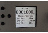
Measurements of 10 MHz Signal Generator DDS (150210-1 v1.1)
Levels of sine signals at different frequencies (P2 at fixed position):
Approximately 0.5 Vpp at 1 kHz:
f A [Vpp] Display [Vpp]
1 kHz 0.488 0.54
10 kHz 0.492 0.54
100 kHz 0.495 0.54
1 MHz 0.546 0.58
2 MHz 0.668 0.72
3 MHz 0.833 0.90
4 MHz 0.986 1.10
5 MHz 1.114 1.32
6 MHz 1.231 1.52
7 MHz 1.347 1.74
8 MHz 1.398 1.88
9 MHz 1.444 1.96
9.9 MHz 1.481 2.00
Approximately 5 Vpp at 1 kHz:
f A [Vpp] Display [Vpp]
1 kHz 4.883 4.90
10 kHz 4.920 4.90
100 kHz 4.946 4.90
1 MHz 4.973 5.02
2 MHz 5.164 5.30
3 MHz 5.417 5.80
4 MHz 5.688 6.26
5 MHz 5.957 6.68
6 MHz 6.105 7.04
7 MHz 6.288 7.34
8 MHz 6.227 7.52
9 MHz 6.196 7.54
9.9 MHz 6.114 7.58
Approximately 15 Vpp at 1 kHz:
f A [Vpp] Display [Vpp]
1 kHz 14.69 14.74
10 kHz 14.60 14.72
100 kHz 14.59 14.72
1 MHz 14.59 14.74
2 MHz 14.18 14.78
3 MHz 13.92 14.54
4 MHz 13.23 14.10
5 MHz 12.51 13.64
6 MHz 11.77 13.20
7 MHz 11.05 12.80
8 MHz 10.09 12.36
9 MHz 9.317 11.72
9.9 MHz 8.694 11.16
Measured at the input of potentiometer P2 (sine):
f A[Vpp]
1 kHz 1.523
10 kHz 1.532
100 kHz 1.540
1 MHz 1.549
2 MHz 1.527
3 MHz 1.510
4 MHz 1.475
5 MHz 1.446
6 MHz 1.395
7 MHz 1.370
8 MHz 1.307
9 MHz 1.269
9.9 MHz 1.242
Maximum output voltage (load 10 MΩ): 16 Vpp (sine)
16 Vpp (triangle)
18 Vpp (square)
Supply current -15 V: 21 mA
120 mA (50 Ω load with maximum negative output voltage)
Supply current +15 V: 58 mA
166 mA (50 Ω load with maximum positive output voltage)
Supply current +3V3: 96 mA (sine)
127 mA (10 MHz square)
50 % duty cycle accuracy: 100 Hz – 10 kHz: 3 % (display value 47 %)
10 kHz – 1 MHz: 2 % (display value 48 %)
Rise and fall time (80 %): 100 ns (both)
In Plot A a 1 MHz square wave at the output is shown with almost maximum level. Bandwidth is limited by voltage divider R25/P2. The signal on P2 is virtually the same (Plot B). In Plot C the output signal of IC6B is shown. Obviously there’s quite some parasitic capacity after R25. But compensating with just a capacitor parallel to R25 is not enough. The inductance of P2 must also be compensated and the whole compensation would become rather complex.
Bill of materials
Resistor
R1 = 220 Ω, 1 %, 0W75, SMD 2010
R2,R22,R23,R37 = 1 kΩ, 1 %, 0W125, SMD 0805
R3 = 1 kΩ, 1 %, 0W1, SMD 0603
R5-R12,R30,R31,R36 = 10 kΩ, 1 %, 0W125, SMD 0805
R13 = 6k8, 1 %, 0W125, SMD 0805
R14,R15 = 200 Ω, 1 %, 0W125, SMD 0805
R16,R19,R25 = 910 Ω, 1 %, 0W125, SMD 0805
R17,R20 = 1k2, 1 %, 0W125, SMD 0805
R18,R26 = 2k0, 1 %, 0W125, SMD 0805
R21,R24 = 499 kΩ, 1 %, 0W125, SMD 0805
R27 = 220 Ω, 1 %, 0W125, SMD 0805
R28 = 10 Ω, 1 %, 0W125, SMD 0805
R29 = 10 kΩ, 1 %, 0W1, SMD 0603
R32,R33 = 100 Ω, 1 %, 0W75, SMD 2010
P1 = 10 kΩ, 5 %, 2 W, 10-turn potentiometer
P2 = 1 kΩ, 5 %, 2 W, 10-turn potentiometer
Capacitor
C1,C3,C4,C12,C13,C14,C16,C17,C19,C20,C26,C27,C28,C29,C31 = 100 nF, 10 %, 50 V, X7R, SMD 0603
C2,C5 = 10 µF, 10 %, 16 V, X7R, SMD 1206
C6,C7 = 470 nF, 10 %, 25 V, X7R, SMD 0603
C11 = 1 µF, 10 %, 16 V, X7R, SMD 1206
C15 = 10 nF, 10 %, 50 V, X7R, SMD 0603
C18 = 10 pF, 5 %, 50 V, C0G/NP0, SMD 0603
C21 = 100 pF, 5 %, 100 V, C0G/NP0, SMD 0805
C22,C23 = 220 µF, 20 %, 25 V, radial, lead spacing 3.5 mm, diam 8 mm max. (EEU-FM1E221, Panasonic)
C24,C30 = 100 nF, 10 %, 50 V, X7R, SMD 0805
Semiconductor
IC1 = ADUC7024BSTZ62, SMD LQFP-64
IC2 = AD8032ARZ, SMD SOIC-8
IC3 = AD9834BRUZ, SMD TSSOP-20
IC4 = 75 MHz oscillator (FXO-HC736R-75, Fox Electronics), SMD 7 x 5 mm
IC5,IC6 = AD8042ARZ, SMD SOIC-8
IC7 = ADG779BKSG-REEL7, SMD 6-Lead SC-70
IC8 = AD811ANZ, DIP-8
IC9 = OP1177ARZ, SMD SOIC-8
IC10,IC11 = ADR1581ARTZ-REEL7, SMD SOT-23-3
Other
K1 = Socket, 0.5mm, 1.5mm stack, 10way, DF23C-10DS-0.5V(51), Hirose (HRS)
K2,JP1,JP2 = 1x2 pin header, vertical, pitch 2.54mm
K3 = 2x3 pin header, vertical, pitch 2.54 mm
K4 = 1x4 pin header, vertical, pitch 2.54mm
K5 = BNC 50 Ω, Straight Bulkhead Jack, Panel mount (5-1634504-1, TE Connectivity)
S1-S8 = 6 mm tact switch, actuator length 4.9 mm, 24V/0.05A, SPST-NO, Black
Socket, DIP, 8way (08-3518-10, Aries)
Misc.
Aluminum enclosure, Hammond 1455T1601, 165x160x51.5 mm
Optional EMI/EMC filter, Inlet, IEC, 250 VAC/4 A (RIS0422H2, Roxburgh)
Knob, black, 16 mm, shaft diam. 6.35 mm
PCB 150210-1 v1.11
Additional measurements (2-9-2015):
We performed some additional distortion plus noise measurements (THD+N):
Load 100 kΩ, Bandwidth > 500 kHz
1 V, 1 kHz 0.12 %
0.09 % (B = 22 kHz)
5 V, 1 kHz 0.1 %
0.09 % (B = 22 kHz)
1 V, 10 kHz 0.1 %
0.09 % (B = 80 kHz)
5 V, 10 kHz 0.09 %
0.08 % (B = 80 kHz)
1 V, 100 kHz 0.1 %
5 V, 100 kHz 0.08 %
S/N (referred to 1 V, P2 at minimum, 0 VDC) 72 dB
73 dB (B = 22 kHz)
We also recorded some plots with our Audio Precision Analyzer:
Plot D shows a FFT up to 130 kHz of a 1 V 1 kHz signal (fundamental suppressed). THD+N is mainly caused by the harmonics of the signal. Some mains related (50 Hz) components are visible but are close to the noise floor.
Plot E shows a FFT up to 130 kHz of a 1 V 10 kHz signal (fundamental suppressed). THD+N is also mainly caused by harmonics of the signal.
Plot F shows a FFT up to 130 kHz of the output with P2 set at minimum setting. The 1 kHz signal is still visible due to the fact that the potentiometer is not a perfect short circuit when set to minimum level. The higher noise floor is obviously caused by the AD811 in the output stage.
For comparison we also measured the prototype of Theodorou. Potentiometer P2 has more ‘leakage’ at the minimum setting, clearly visible in plot G. The noise floor looks pretty much the same as our prototype.
Diskussion (4 Kommentare)