
Audio DAC for RPi - Networked Audio Player using Volumio [160198]
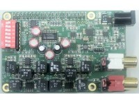
This is an Audio DAC designed for the Raspberry Pi. Using app Volumio it can be used as a stand alone networked Audio Player or operated thru a WebUI.
Searching for a small stand-alone networked audio player with a touch screen mostly big consumer amplifiers are found. The one’s with network support have no touch screen or are very expensive. If space and mobility is an issue these are not suitable. So, why not build one yourself. Luckily there are many who already did. A good start is to look for applications that use a raspberry pi. DACs with good quality are already on the market. But since we want to build de audio player ourselves, we designed an audio DAC for the raspberry pi using first class parts. In the past we designed High End DACs for normal use. ICs from Burr Brown (now Texas Instruments) were and still are among the best. We had good experiences with DACs made by Burr Brown and so the choice was easy to use one of their top models, the PCM1794A. It is a 24 bit DAC , can handle sample rates up to 200 kHz and has a built-in 8x oversampling filter.
Power supplies
The PCM1794A (IC1) requires two different power supply voltages. +3.3 V for the digital part and +5 V for the analog part. Later on we will explain why we increased this supply voltage to +5.2 V (still within recommended operating range!). We could use the RPi power supplies available on the GPIO Expansion connector but these are very noisy. We need to make an independent +3.3 V and +5 V. Another option is to use the power supply of the DAC to supply the RPi. But that would mean degrading the power supply of the DAC. Downside of keeping the power supplies separate is two DC adapters are needed. To avoid having to use a third power supply for the I/V-converter and analog output filter a negative power supply is derived from the +5 V. The positive supply voltage for the analog output section is set to 4.74 V using a low noise regulator and the negative power supply is also derived from the +5.2 V power supply using a special Low-Noise Regulated Switched Capacitor Voltage Inverter: the LM27761 (IC8). As the name explains it uses switched-capacitor techniques to invert the input voltage followed by a linear low noise regulator to create a stabilized negative supply voltage. In our case the output voltage is set to -4.81 V by divider R30/R31 (Vout = -(R30/R31 + 1) * 1.22 V). The IC can supply up to 250 mA and the IC measures only 2 x 2 mm. It’s size and operating frequency of 2 MHz means very little noise is introduced. Two ultralow-noise positive linear regulators of type TPS7A4901 are used for the +3.3 V (IC9) and +4.74 V (IC7) ensuring the best power supply quality for the DAC and filters. The maximum output current is 150 mA The output voltages (Vout = (R28/R29 + 1) * 1.185 V) are set to +4.74 V by divider R28/R29 and +3.3 V by divider R32/R33.
Ultralow-noise low-dropout voltage regulator TPS7A4700 is used to generate the +5.2 V main power supply. It can deliver 1 A output current and has a low drop-out voltage of 307 mV (at 1 A). It has internal resistors so the output voltage can be set by connecting specific pins to ground. If connected to ground each pin adds a voltage to the output. The minimum voltage is the reference voltage of 1.4 V. To get +5.2 V pins 6, 10 and 11 are connected to ground: Vout = 1.4 + 3.2 + 0.4 + 0.2 V = 5.2 V. The slightly higher output voltage was chosen to ensure the maximum undistorted output voltage of the filter stages can be 1 V. Conventional maximum output voltage is often 2 VRMS but that would require rail to rail opamps or a higher supply voltage. A design criteria was to avoid additional power supply voltages. Most rail-to-rail opamps don’t have the specifications that special high quality audio opamps have. We used two dual opamps type LME49720 for the I/V-converters and two single opamps type LME49710 for the filters. Although their power supply range is specified ±2.5 V to ±17 V the linear output voltage range measurements have shown the linear output voltage range (at this low power supply voltage) is a about 1.4 V from each supply line. The I/V-converter is the limiting factor here, partially caused by the low resistor values (higher drop across the internal output transistors). This is discussed in the filter section in more detail. This is the reason the original symmetrical power supply voltage of ±4.5 V was increased to +4.74 V and – 4.81 V (the use of E-24 values provide these voltages). Now the maximum (0 dB) output voltage of 1.06 V is undistorted.
The input for the power supply (K7) is protected against wrong polarity by a schottky diode (D1). The voltage drop across the diode is about 0.3 V. At 8 V input voltage the supply current is 124 mA playing at a sample rate of 32 kHz and 184 mA playing at a sample frequency of 192 kHz.
Master clock
Making the audio DAC work we configured Raspbian (operating system of the RPi) for a HiFiBerry DAC. If this is done correctly I2S serial bus signals (Inter-IC Sound) are available on the GPIO Expansion connector. Official names of the signals are continuous serial clock SCK (or bit clock BCLK/BCK), word select WS (or left-right clock LRCLK/LRCK) and serial data SD (or SDATA/DATA and many more). Originally not part of the I2S standard is a master clock needed to synchronize devices. The master clock is missing on the expansion connector and so our circuit has to generate one. For this purpose we added a frequency multiplier with integrated PLL. The ICS570BILF from IDT has a zero delay buffer which means the rising edges of input and outputs are perfectly aligned. The multiplication can be set from 0.5x to 32x by two three level inputs (S0/S1). Output range of CLK is according to the AC Electrical Characteristics 10 to 170 MHz. We set the multiplication to 6x using the CLK/2 output and connected it to the feedback input. This configuration has the best input range setting. According to the Clock Multiplier Decoding Table and M/M setting in the datasheet setting both S0 and S1 to M (unconnected) the input range is 2.5 to 12.5 MHz and the output range is 15 to 75 MHz. This would mean that a 32 kHz sample frequency track should not be able to play, yet is does and it does so perfectly. But there is a bigger problem. To test the audio DAC all kinds of 32 bit wave files were used: stepped sine, stepped amplitude, single tone and IMD with sample frequencies from 32 kHz to 192 kHz. Doing tests with a few 24 bit wave files gave exact same results. So next to do were tests and measurements with 16 bit waves and big surprise: no output signal! What the f***…Well it took it a long time to come to the conclusion that although the datasheet states the PCM1794A supports 16 and 24 bit audio, it does not in the I2S mode. The only indication I found in the datasheet (SLES117B –AUGUST 2004–REVISED DECEMBER 2015) was in Figure 22. Audio Data Input Formats. The timing diagram for I2S Data Format mentions Audio Data Word = 24-Bit. And there’s no other I2S diagram. The audio player used by Volumio halves the serial clock and data bits when the audio data is 16 bit. Setting the master clock to higher frequencies doesn’t help. Does this mean 16 bit audio is not supported in our setup. Well yes and no. Playing the song directly doesn’t work but luckily the version of Volumio we used (1.55) still has an option for sample rate conversion (three quality settings). A variety of sample rates and bit combinations are available. This feature should be implemented in a next update of Volumio 2 (version 2.041 of 12-12-2016 still doesn’t, but then Volumio 2 has internet radio, and plug-ins…).
Table 1:
fs[kHz] bits BCK[MHz] S0 S1 * SCK[MHz] output signal
32 24/32 2.048 M M 6 12.288 yes
44.1 24/32 2.8224 M M 6 16.9344 yes
48 24/32 3.072 M M 6 18.432 yes
96 24/32 6.144 M M 6 36.864 yes
192 24/32 12.288 M M 6 73.728 yes
32 16 1.024 M M 6 unstable no
44.1 16 1.4112 M M 6 unstable no
48 16 1.536 M M 6 9.216 no
96 16 3.072 M M 6 18.432 no
192 16 6.144 M M 6 36.864 no
M (half the supply voltage, unconnected)
16 bit audio data can be the reason there’s no sound using internet radio in Volumio 2. Use resampling to 24 bit to get the music playing. If anyone has a solution how to keep the I2S bus in 32 bit data mode permanently please let us know.
Other master clock frequencies can be set by S0 and S1 located on the bottom side by using 0 Ω resistors (0805) or thin wires. Don’t connect all three pads of JP1 and JP2. This will short circuit the +3.3 V power supply.
PCM1794ADB
The DAC has a built-in 8x oversampling digital filter and is compatible with sampling frequencies from 10 to 200 kHz. The datasheet also states ‘Accepts 16-Bit and 24-Bit Audio Data’ but apparently not in I2S mode. I’m not going to duplicate the contents of the datasheet but instead walk through the schematic. The I2S signals are connected through four 22 Ω resistors (R22..R25) to prevent RF noise of these high frequency signals getting to the analog side of the DAC. At a sampling rate of 192 kHz our master clock is almost 74 MHz! The hardware select lines (MONO, CHSL, DEM, MUTE, FMT0, FMT1, RESET) are connected to a 7way DIP switch and a 7way 47 kΩ resistor array used as pull-ups. This makes changing settings very easy. The zero output (pin 13), active when the audio input data in the L-channel and the R-channel is continuously zero for 1024 LRCKs in the PCM mode (or 1024WDCKs in the external filter mode), is connected to LED1 indicating the absence of data. The minimum output level of the ZERO output at a current of 2 mA is according to the datasheet 2.4 V. This is enough for a green led. In our prototype the output voltage was 3.09 V and the led current 4.3 mA. The output current reference bias pin 20 is connected to a 10 kΩ resistor. This is according to the typical application schematic and evaluation board but other than the value no information is given. The left and right channel internal bias decoupling pins (VCOML/VCOMR) are decoupled by 10 µF electrolytic capacitors but again no information is given. To decouple the power supplies we used aluminum polymer capacitors (C19,C23,C25,C27) because of their low ESR (40 mΩ @ 100 kHz). Downside of these capacitors is the relatively high leakage current of 100 µA maximal. Since it is unclear if this leakage current will influence the internal bias setting two normal electrolytic capacitors are used (1.06 Ω @ 100 kHz and 4 µA leakage current). For those who like to experiment footprints of all electrolytic capacitors are designed to hold 2 to 2.5 mm pitch capacitors with a maximum diameter of 6.3 mm. The 47 nF ceramic decoupling capacitors of the power supply pins (C22,C24,C26) are size 1206 with X7R dielectric. Would the use of NP0/C0G dielectric improve performance?
The output filter
Although sampling artifacts are largely suppressed by the 8x digital oversampling filter there are still high frequency components present. A reconstruction filter is used to suppress them. But since we’re using an 8x oversampling filter its task is foremost suppressing the higher frequencies above half the sample frequency. A 3rd order Butterworth is used. The I/V-converters IC2/IC3 are part of the filter. The cut-off frequency is 64.5 kHz. At a sampling frequency of 44.1 kHz the 8x frequency component of 352.8 kHz is suppressed by more than 40 dB. At a sampling frequency of 192 kHz the 8x frequency component will be suppressed by approximately 80 dB. The chosen cut-off frequency is of course a compromise between sufficient filtering at lower sampling frequencies and low frequency bandwidth of the audio signal at the higher sampling frequencies. The filter bandwidth is now more than three times the human hearing range. The DAC has balanced current outputs so an external filter can be used. To convert these balanced currents to a single ended output signal first an I/V-converter per output is needed. The two voltages of IC2A/IC2B (IC3A/IC3B) are followed by a 2nd order filter stage configured as a differential to single ended amplifier. IC4 for the left channel and IC5 for the right channel. The topology is a differential multiple feedback filter. Combined with the filtering of the I/V-converter the total filter characteristic is a 3rd order Butterworth filter. The filter was calculated with exact E-12 values for the capacitors and theoretical values for the resistors. The resistor values were rounded to E-24 values.
In our prototype the balanced output currents were just 5.8 mA (no signal) instead of the 6.2 mA according to the datasheet. If the tolerance is this big (6.5 %) there’s also the possibility the current is equally higher. Hopefully this doesn’t mean the I/V-converter is clipping if a full-scale signal is applied. Not only is the center current lower but the full-scale peak-peak current is also proportionally lower. The measured output voltages of the I/V-converters were 2.08 in one channel and 2.06 in the other. Peak-peak voltage was about 2.7 Vp-p. Maybe tweaking R20 is an option in case the signals are clipping at full-scale. We haven’t tried. Another option to use a higher symmetrical power supply for the filter. In that case remove 0 Ω resistors R26 and R27 and connect the external power supply to K6.
For the output stage a multiple feedback filter is used since it can easily be extended to also function as differential to single ended converter. If familiar with a standard multiple feedback filter transforming it to one with a differential input is simple. Just mirror the circuit connected to the inverting input and place it at the non-inverting input. The resistor and capacitor connected to the output are connected to ground. That’s it, well almost. If you look at the circuit you see that there’s only one capacitor (C9/C14) were you would expect two capacitors connected to ground. The original two capacitors can be combined to one with only half the value. The bigger the value of high quality capacitors like we used in the filter the higher the cost. By replacing two capacitors by one smaller capacitor per channel we save some money but more importantly we save space. The idea was to keep the PCB of the DAC exactly the same size as the RPi PCB and components should only be mounted on the top side. To limit the output voltage to 1 V the filter has to attenuate the differential signal of the I/V-converters. Gain of IC4/IC5 is 0.56, set by the ratio of R6/R5 and R9/R8. DC output offset is only in the mV range. -1.6 mV in one channel and +1.3 mV in the other channel. The common mode voltage of both I/V-converters per channel is suppressed by IC4 and IC5. The single ended output signal is made available on PCB mounted RCA connectors K1 and K2 through connectors K3 and K4. A shunt jumper on K3/K4 can be used to make a direct connection to the RCA connectors. K3 and K4 can also be used to connect a stereo potentiometer to have a simple volume control. The DAC itself has no volume control. Volumio can change volume by software but then resolution is lost. This would seriously compromise sound quality and is not really an option. Another possibility is to insert a hardware volume control like a PGA2311 (another PCB) and change volume by remote control (work in progress). Recently there is plug-in available for Volumio 2 to connect push buttons to the RPi to control basic functions. These can be added to the other PCB.
The symmetrical analog power supply for the filter and the I/V-converter is decoupled from the digital power supplies by a common-mode choke and RF inductors for each channel.
PCB
Only a single power supply of 7 to 8 V is needed (K7). The RPi works on a separate 5 V! Any higher will cause more dissipation in the voltage regulator IC10 but 9 or 12 V are also possible. The DC power connector jack and RCA phono jacks are on the same side. DIP switch S1 is on the opposite side of the PCB. This is the spot on the RPi 3 where the WiFi antenna is located. The 40-pin GPIO Stacking Header K5 is mounted on the bottom side. Don’t put the plastic body of the header against the PCB but keep it 1 to 1.5 mm from the PCB and keep the distance equal (perfect parallel to the PCB) so it will fit on the corresponding connector on the RPi without a problem. Cut the protruding pins on the bottom side of K1, K2, K3, K4, K6 and K7 as short as possible to avoid short circuits occur with the metal cases from the network and USB connectors on the RPi. Maybe place something insulating in-between. We used four M2 screws of sufficient length to act as spacers (and 12 nuts). The standard spacers are not long enough. The footprint for the capacitors that are part of the filter is designed so 3 different types of capacitors can be used (C1, C2, C5, C6, C9, C10, C11, C14, C15, C16). SMD 0805 capacitors can be used but also standard through hole capacitors with 5 mm spacing. We strongly recommend the use of 1 % polystyrene capacitors for best performance (see BOM). These capacitor have the pins placed diagonally. The number 1 pins of all ICs are marked with a white dot next to it. The dot of IC7 is a bit hard to see, it is half absorbed by C38. Because there is not enough space to place the designators of all 0805 resistors and 0805 and 1206 capacitors next to the components they are placed inside the component. This means they will not be visible on the PCB. If the components are soldered by hand (hot air or oven) use an enlarged print out of the top overlay to place all SMD at the right place. Many 0805 components are not easily replaced once the through hole components are mounted! Through hole components should be mounted last. Jumpers JP1 and JP2 are located at the bottom. But by default these can be left open (SCK = 6 x BCK). The RCA Phono connectors are types from Switchcraft and have two connection closer together than more standard 10 mm versions. If other types are used they probably won’t fit!
Place the 3.5” display 17 mm above the Audio DAC. Don’t push the connector all the way through. The connector should make sufficient contact. If doubtful use another standard size stacking header and place the display higher. The 26way socket of the display will then be at a distance of about 3,5 mm from the Audio DAC PCB. 17 mm M2.5 standoffs can be used (Ettinger 05.12.173, Farnell 1466854) to secure the Audio DAC on top of the Raspberry Pi.
Volumio 1.55
The following text is a step-by-step description how to install Volumio 1.55 on a Raspberry Pi 3 (if the links are still valid and not updated to Volumio 2) in combination with a 480x320 3.5” LCD to work as a stand-alone music player
First install a copy of the Raspbian image from https://www.raspberrypi.org/downloads/raspbian/ on a Micro SD Card of at least 8 GB. We used 2016-09-23-raspbian-jessie.img. The 3.5” LCD we used comes with a preinstalled Raspian image but we strongly recommend not to use it. This image eventually produced errors (language incompatibilities and more)
Connect a monitor (HDMI), mouse and keyboard
After start-up has finished open a terminal and run:
sudo apt-get update
sudo apt-get upgrade (be patient, this may take a while)
sudo raspi-config (to extend the partition to the full size of the micro SD card and maybe change the keyboard layout to your country, default is English UK)
sudo rpi-update (this updates the firmware of the Raspberry Pi to the latest version)
sudo reboot (to reboot and reactivate the new firmware)
sudo apt-get install midori (an internet browser we know how to start full screen)
Following instructions to disable the screensaver are often given but didn’t work.
sudo nano ~/.config/lxsession/LXDE-pi/autostart it should contain the following lines:
#@xscreensaver -no-splash
@xset s off #disable screensaver
@xset -dpms
@xset s noblank #disable screensaver blanking
@unclutter -idle 0 #disable mouse pointing
midori -e Fullscreen -a http://localhost
Another instruction that should disable the screensaver permanently (worked for us):
sudo nano /etc/lightdm/lightdm.conf and add in the [SeatDefaults] section the following command:
xserver-command=X -s 0 -dpms
sudo apt-get remove --purge minecraft-pi –y (not needed, remove application)
sudo apt-get remove --purge wolfram-engine –y (not needed, remove application, saves space)
sudo reboot (alt-F4 to close midori)
sudo apt-get install alsa-utils mpd mpc minidlna usbmount ntfs-3g -y
sudo nano /etc/mpd.conf comment the following line with #
bind_to_address "localhost"
sudo apt-get install nginx sqlite3 php5-fpm php5-curl php5-sqlite php5-cli php5-gd php5-imagick -y
sudo apt-get install samba samba-common-bin -y
sudo apt-get install ntfs-3g minidlna autofs -y
sudo nano /etc/auto.master add the following line at the end:
/media/ /etc/auto.ext-usb --timeout=10,defaults,user,exec,uid=1000
sudo mkdir /var/www (probably exists already)
sudo mkdir /mnt/disk1
sudo mkdir /mnt/disk2
sudo mkdir -p /mnt/NAS
sudo mkdir -p /mnt/USB
sudo ln -s /mnt/NAS /var/lib/mpd/music/NAS
sudo ln -s /mnt/USB /var/lib/mpd/music/USB
sudo git clone https://github.com/volumio/Volumio-WebUI.git /var/www if next error appears:
fatal: destination path ‘/var/www’ already exists and is not an empty directory.
sudo rm -r /var/www (to delete all contents in /var/www and try again)
sudo chmod 775 /var/www/_OS_SETTINGS/etc/rc.local
sudo chmod 755 /var/www/_OS_SETTINGS/etc/php5/mods-available/apc.ini
sudo chmod -R 777 /var/www/command/
sudo chmod -R 777 /var/www/db/
sudo chmod -R 777 /var/www/inc/
sudo cp -var /var/www/_OS_SETTINGS/etc /
cd /var/lib/mpd/music ; sudo ln -s /mnt/disk1/Music
sudo ln -s /mnt/NAS /var/lib/mpd/music/NAS
sudo ln -s /mnt/USB /var/lib/mpd/music/USB
sudo reboot
At this stage the LCD is still not used, just the HDMI output.
To use the 3.5” display from Waveshare, copy the driver on the CD (in our case the file was called LCD-show-160520.tar.gz) to a directory on the Raspberry Pi. Easiest way to do this is the use of thumb drive. Follow the instruction in the user manual on the CD. It states to run ‘tar xvf LCD-show.tar.gz’.
But of course use the correct path and filename and then run (depending on the location you copied the driver file to):
tar xvf /home/pi/Documents/LCD-show-160520.tar.gz and then run
sudo ./LCD35-show
The system will reboot and Volumio should appear in full screen on the LCD. If you still want to use the Raspberry Pi for other purposes pressing F11 will leave full screen and the Desktop is accessible. Pressing F11 again will put Midori in full screen again (if it’s the active window). Adding/changing contents to a location in Volumio to the library requires a reboot before it becomes visible and accessible.
Because the installation of the LCD overwrites or changes /boot/config.txt we save enabling hifiberry to last. Add the following lines to the file /etc/modules:
snd_soc_bcm2708
bcm2708_dmaengine
snd_soc_hifiberry_dac
Configure ALSA
Create /etc/asound.conf with the following content:
pcm.!default {
type hw card 0
}
ctl.!default {
type hw card 0
}
Enable I2S in /boot/config.txt
Uncomment or add the line:
dtparam=i2s=on
Add line:
dtoverlay=hifiberry-dac
If finally everything works there’s one minor issue. The Menu item ‘Turn off’ is outside the screen on the LCD. To properly powering down the player is either by WebUI on an external device or through the use of an to the RPi attached keyboard and mouse. Getting to know Volumio will prove easy. To get the first track playing after power up one has to push play 3 or 4 times…!?
Measurements
Laboratory Power supply 8 V, 10 kΩ connected to both outputs
S1-1 = L (De-emphasis for 44.1 kHz disabled)
S1-2 = L (Digital Filter Roll Off Sharp)
S1-3 = L (Monaural mode disabled)
S1-4 = L (Mute off)
S1-5 = L, S1-6 = L (I2S mode)
S1-7 = H (Reset disabled)
Supply current (K7) no data 120 mA
32 kHz 127.5 mA
44.1 kHz 131.7 mA
48 kHz 133 mA
96 kHz 149.5 mA
192 kHz 182.1 mA
THD+N
Sampling frequency 48kHz 96 kHz 192 kHz
1 kHz B = 22 kHz 0.0008 % 0.0009 % 0.0013 %
B = 80 kHz 0.0028 % 0.0012 % 0.0014%
7 kHz B = 22 kHz 0.00095 % 0.0011 % 0.0013 %
B = 80 kHz 0.003 % 0.0014 % 0.0016 %
IMD
50 Hz : 7 kHz = 4 : 1 0.0014 % 0.002 % 0.0036 %
Bandwidth analog filter 64.5 kHz
Maximum sine wave 1.06 V
We also recorded some plots with our Audio Precision Analyzer
Plot A shows amplitude as a function of frequency using a stepped sine wave with 70 frequencies at full-scale and a sample frequency of 192 kHz. The upper (green) curve is recorded with sharp roll off mode. The lower curve (cyan) is recorded with the digital filter in slow roll off mode. The cut-off frequency is 63.5 kHz (theoretically 64.5 kHz). At 90 kHz amplitude is -9.2 dB for the sharp roll off mode and -12.3 dB for slow roll off mode. At 45 and 51 kHz the amplitudes are the same for both, -0.5 and -1 dB respectively.
Plot B shows channel separation as a function of frequency. The upper curve (green) is the crosstalk from the left channel on the right channel. This curve is slightly higher than the other way around (cyan curve is crosstalk from right to left). The connection to the RCA output connectors are not of equal length. The track for the right output signal is longer and therefore the crosstalk from left to right is higher. But considering the compact design this is pretty good. The levels are in the µV range. Although measurement is done with a sharp band filter and measurements are averaged noise at these low levels makes the curves a bit jumpy. This measurement was performed using two stereo stepped sine waves with 100 frequencies and a sampling frequency of 96 kHz with the other channel digital 0.
Plot C shows total harmonic distortion plus noise as a function of frequency at sampling rates of 48, 96 and 192 kHz. The bandwidth is 80 kHz for all three measurements. The THD+N at a sampling frequency of 48 kHz is much lower if we use a bandwidth of 22 kHz. If we look at the frequency spectrum we see a increase in noise just outside the audio bandwidth. We suspect this is due to noise shaping at 48 kHz. This increase in noise is absent in the spectra of 96 and 192 kHz sampling frequency.
Plot D shows the FFT analysis of a 1 kHz full-scale sine wave at a sampling frequency of 32 kHz. Noticeable is the increase in noise just above the audio bandwidth (noise shaping?). THD+N at a bandwidth of 22 kHz is just 0.0007 % (0.012% at 80 kHz). A lot of spurious frequencies are visible caused by the Raspberry Pi just underneath (common mode noise from the power supply of the RPi, a simple AC adapter with USB output), surrounding equipment at the test setup and maybe jitter from the master clock. But -120 dB means 1 µV! The second and third harmonic are barely visible (around -120 dB)
Plot E shows the FFT analysis of a 1 kHz full-scale sine wave at a sampling frequency of 44.1 kHz. The high frequency noise is less than the 32 kHz plot. THD+N at a bandwidth of 22 kHz is 0.0006 % (0.0038 % at 80 kHz). The other frequencies are not that different and look very much like the 32 kHz plot. The second and third harmonics are a bit more prominent, -117 and -118 dB respectively. This amount to a harmonic distortion (just the two harmonics without noise) of only 0.00019 %.
Plot F shows the FFT analysis of a 1 kHz full-scale sine wave at a sampling frequency of 48 kHz. Best guess is with higher sampling frequency more RF noise is picked up at the analog side of the DAC. But don’t let the plot fool you. THD+N at a bandwidth of 22 kHz is only 0.0008 % (0.0028 % at 80 kHz). The high frequency noise is a little lower compared to the 44.1 kHz plot.
Plot G shows the FFT analysis of a 1 kHz full-scale sine wave at a sampling frequency of 96 kHz. The high frequency noise is gone and a instead a highly suppressed sampling frequency is visible. The harmonics have increased but none the less THD+N at a bandwidth of 22 kHz is 0.0009 % (0.0012 % at 80 kHz).
Plot H shows the FFT analysis of a 1 kHz full-scale sine wave at a sampling frequency of 192 kHz. The sampling frequency is outside the range of our Audio Precision analyzer. Distinct difference is the increase in amplitude of the harmonics which shows clearly in the THD+N of 0.0013 % at a bandwidth of 22 kHz (0.0014 % at 80 kHz). For the most part due to the third harmonic. But THD+N is better than the typical value in datasheet. And our measurement is done at almost a fifth of the output voltage from the datasheet (4.5 V).
The following plots are made using16 bit wave files resampled on the fly, a feature in Volumio 1.55. The same sampling frequencies are used in the 16 bit files as the previous plots and are resampled to 24 bit and a sampling frequency of 96 kHz. As already explained the resampling to 24 bit (or 32) is necessary to play 16 bit files with Volumio.
Plot I shows the FFT analysis of a 16 bit 1 kHz full-scale sine wave at a sampling frequency of 32 kHz resampled to 24 bit/96 kHz. At a first glance the spectrum looks ‘cleaner’ but not really. The noise floor and the harmonics are higher. THD+N at a bandwidth of 22 kHz is 0.0016 % (0.0019 % at 80 kHz). This value is purely caused by the increase in harmonics (the source is only 16 bit!). Noticeable is the absence of the high frequency noise visible in plot D.
Plot J shows the FFT analysis of a 16 bit 1 kHz full-scale sine wave at a sampling frequency of 44.1 kHz resampled to 24 bit/96 kHz. Numerous intermodulation frequencies but at a lower level than the harmonics and the sudden drop of the noise floor at 20 kHz are clearly different from plot I and caused by the ratio of the two sampling frequencies. THD+N is at a bandwidth of 22 kHz is 0.0017 % (0.002 % at 80 kHz).
Plot K shows the FFT analysis of a 16 bit 1 kHz full-scale sine wave at a sampling frequency of 48 kHz resampled to 24 bit/96 kHz. Due to the lower resolution the harmonic distortion is slightly higher and also the high frequency noise is gone. THD+N at a bandwidth of 22 kHz is 0.002 % (0.0022 % at 80 kHz).
Plot L shows the FFT analysis of a 16 bit 1 kHz full-scale sine wave at a sampling frequency of 96 kHz resampled to 24 bit/96 kHz. Some intermodulation frequencies above 20 kHz are visible now that were not present in plot G. Is this audible? THD+N at a bandwidth of 22 kHz is 0.0016 % (0.002 % at 80 kHz).
Plot M shows the FFT analysis of a 16 bit 1 kHz full-scale sine wave at a sampling frequency of 192 kHz resampled to 24 bit/96 kHz. Surprisingly the number of intermodulation frequencies are few. Distortion is mainly defined by harmonics. THD+N at a bandwidth of 22 kHz is 0.0015 % (0.0018 % at 80 kHz).
Bill of materials
Resistor
R1,R2,R3,R4,R7,R10,R13,R16 = 360 Ω, 125 mW, 1 %, SMD 0805
R5,R8,R11,R14,R34 = 1 k, 125 mW, 1 %, SMD 0805
R6,R9,R12,R15 = 560 Ω, 125 mW, 1 %, SMD 0805
R17,R18 = 47 Ω, 125 mW, 1 %, SMD 0805
R19 = 270 Ω, 125 mW, 1 %, SMD 0805
R20 = 10 k, 125 mW, 1 %, SMD 0805
R21 = 47k, Resistor Array 7 bussed, 125 mW, 2 %
R22,R23,R24,R25 = 22 Ω, 125 mW, 1 %, SMD 0805
R26,R27 = 0 Ω, 125 mW, 1 %, SMD 0805
R28 = 300 k, 125 mW, 1 %, SMD 0805
R29,R33 = 100 k, 125 mW, 1 %, SMD 0805
R30 = 150 k, 125 mW, 1 %, SMD 0805
R31 = 51 k, 125 mW, 1 %, SMD 0805
R32 = 180 k, 125 mW, 1 %, SMD 0805Ω
Capacitor
C1,C2,C5,C6,C9,C14 = 6n8, 63 V, 1 %, polystyrene, EXFS/HR 6800PF +/- 1%, LCR Components
(alternative lead spacing 5 mm or 0805)
C3,C4,C7,C8,C12,C13,C17,C18,C29,C34,C35 = 100 n, 50 V, 10 %, X7R, SMD 0805
C10,C11,C15,C16 = 2n2, 63 V, 1 %, polystyrene, EXFS/HR 2200PF +/- 1%, LCR Components
(alternative lead spacing 5 mm or 0805)
C19,C23,C25,C27 = 10µF, 35V, 0.04Ω, diam. 6.3 mm max., lead spacing 2/2.5 mm
870055673001 (WCAP-PTHR Series), Würth Elektronik
C20,C21 = 10 µF, 63V, 1.06 Ω, diam. 6.3 mm max., lead spacing 2/2.5mm
UPM1J100MDD, Nichicon
C22,C24,C26 = 47 n, 50 V, 10 %, X7R, SMD 1206
C28 = 10 n, 50 V, 10 %, X7R, SMD 0603
C30,C31,C32,C33,C36,C37,C40,C41,C43,C44,C46,C47,C48,C49,C52,C53 = 4µ7, 25 V, 10 %, X5R, SMD 0805
C38,C39,C50,C51 = 10 n, 50 V, 10 %, X7R, SMD 0805
C42 = 2µ2, 10 V, 10 %, X7R, SMD 0805
C45,C55 = 1 µ, 16 V, 10 %, X7R, SMD 0805
C54 = 47 µF, 16 V, 20 %, X5R, SMD 1210
C56,C57 = 10 µF, 25 V, 10 %, X5R, SMD 1206
C58 = 47 µF, 16 V, 10 %, tantalum, SMD Cased C (2312), TR3C476K016C0350, Vishay
Inductor
L1,L2,L3,L4,L6,L7 = 600 Ω @ 100 MHz, 0.15 Ω, 1.3 A, SMD 0603, BLM18KG601SN1D, Murata
L5 = ACM4520-231-2P-T, 2 x 0.05 Ω, 230 Ω @ 100 MHz, 2.6 A, SMD, TDK
Semiconductor
D1 = PMEG6030EP, 60 V, 3 A, SMD SOD-128
LED1,LED2 = Led, green, low-power, SMD 0805
IC1 = PCM1794ADB., SMD SSOP-28
IC2,IC3 = LME49720MA/NOPB, SMD SOIC-8
IC4,IC5 = LME49710MA, SMD SOIC-8
IC6 = ICS570BILF, SMD, SOIC-8
IC7,IC9 = TPS7A4901DGNT, SMD MSOP-8
IC8 = LM27761DSGT, SMD WSON-8
IC10 = TPS7A4700RGWT, SMD VQFN-20
Other
K1 = RCA phono jack, white, PCB mount, right angle, gold, PJRAN1X1U02AUX, Switchcraft
K2 = RCA phono jack, red, PCB mount, right angle, gold, PJRAN1X1U03AUX, Switchcraft
K3,K4,K6 = 3-way pinheader, vertical, pitch 2.54 mm
K3,K4 = Shunt jumper, 2.54 mm spacing
K5 = 40-pin GPIO Stacking Header - 2x20 Female - Extra Tall
K7 = DC Power Connector, Jack, 3 A, 1.95 mm, Lumberg NEB 21 R
S1 = 7-way DIP switch
4 M2.5 17 mm standoffs
4 M2.5 6mm screws
4 M2.5 nuts
Misc.
PCB 160198-1 v1.1
Updates vom Autor