
100 MHz - 3 GHz RF comb generator
This is a very simple, but effective comb generator that, once driven with a 100 MHz signal, is capable to produce regularly spaced harmonics even beyond 3 GHz. Inexpensive and useful for many RF tests and experiments.
Introduction
In these days, after making some experiments with pulse generators, an old idea has come back to my mind: to design and build a 1-18 GHz comb generator with an SRD (step recovery diode), for which I have some suitable microwave devices.
An SRD is a regular silicon diode, optimized to have a controlled storage time, a quite low reverse bias capacitance and a very fast voltage reversal at the end of the storage period: this fast voltage jump, named snap-off, generates a lot of harmonics and is used for frequency multipliers and comb generators.
At this point you may wonder what a comb generator is: it is a circuit that generates many harmonics of a base frequency, all at the same time and with similar amplitudes (although a gradual level decay is unavoidable). Its signal, seen with a spectrum analyzer, looks like a comb (see fig. 4).
Picking up the matter, I realized that doing it right at 18 GHz was not an easy task! Browsing around in search for documentation and design ideas, I discovered that someone succeeded at using the inexpensive BA482 TV band-switching diode as an SRD up to at least 2 GHz: in particular, reference is made to [1]. Looking around in the lab, I found several BA282s, which shouldn't be much different from the BA482, so I decided to use them to make some practice working at a lower frequency.
Design considerations
I looked at the comb generator proposed in [1] on page 30, but I preferred to follow the schematic suggested by hp in [2] on pages 8-9, where there are also some simple formulas for sizing the main parts.
Before starting, since the BA282 datasheet obviously didn't contain useful information to use it as an SRD, I decided to make some measurements on the diode. Following the suggestions in [3], I inserted the BA282 in series with a 50 ohm line between my signal generator and oscilloscope (both set with 50 ohm ports) and driving the chain with a rectangular wave having a small duty-cycle: see figs 5-6. I thus obtained the measurement in fig. 7, which provides the important measurement of the storage time (about 16 ns) and shows that the desired snap-off actually takes place: for the latter I measured a rise time of about 1 ns, which is less than the oscilloscope nominal rating of 1.8 ns, so it was almost surely overestimated (and the lower, the better!). At this point I did a few calculations and put together the circuit in figs 1-2-3, which gave me the incredible satisfaction of working on the first try! The spectrum you see in fig. 4 is obtained with +13 dBm input (the maximum of my Marconi 2019A RF generator). The performances seem very respectable, with a good output at 2.9 GHz and probably beyond.
Project details
With reference to the schematic in fig. 1, C1 and C4 are for DC decoupling; additionally, C4 is kept small to attenuate the fundamental signal at 100 MHz and the 1st 3 harmonics, as can be noticed in fig. 4 looking at the leftmost lines.
L2 and D1 are the key components: L2 charges the diode when pushing current in the forward conduction direction, then empties the charge when current reverses. Due to diode threshold, bias and imperfect efficiency, the reverse charge is always less than the forward charge, so emptying the diode takes less time than filling it: the trick consists in having a current close to the maximum peak when the diode snaps-off, so that the high magnetic energy stored in L2 produces a fast and high-voltage spike with the little reverse capacitance of D1 (around 1.25 pF according to the data-sheet). The best point is found by acting on R1, that controls the self-bias due to rectification.
C3 resonates L2 at the input frequency and ensures a return to ground on the left side of L2 for harmonics.
C2 and L1 match the C3-L2 node to 50 ohm.
The circuit must be driven by a sinusoidal generator at 100 MHz with power around +13 dBm (20 mW) to obtain the output of fig. 4. Lower power reduces the output level and the number of harmonics generated. Minimum is around +5 dBm with 4-5 harmonics only.
Probably a higher power up to 20-25 dBm can be applied without destroying the diode, but I haven't tested that yet.
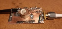
I have mounted the circuit on a small piece of 0.8 mm double-face FR4. With that thickness, 50 ohm lines are 1.4 mm wide, good to put 0805 or 0603 SMD components in line.
I have built traces by removing copper with a cutter, building two short 50 ohm lines for input and output, with cuts for C1 and C4. The output trace terminates on an SMA connector on board edge and is particularly short, just the room for soldering the connector center pin, C4 immediately following, another 2 mm trace as fixing point for D1 and L2.
A small pad, again obtained cutting some copper, hosts the node L1/L2/C3. C3 consists in 2*100 pF capacitors towards ground.
The input 50 ohm line has C1 in line and supports the node R1/C2/L1.
Be careful to keep L1 and L2 at 90° of each other, to avoid coupling.
The diode orientation is not important, only affects the polarity of the self-bias.
Finally, I have short circuited the top and bottom layers almost all around and on the ground of the output SMA connector.
Best tuning requires a spectrum analyzer, but also a simple power meter on the output can do the job. Using a spectrum analyzer, remember to set an input attenuation of at least 20 dB or an external attenuator, because the output signal is quite strong.
References
[1] Matiaz Widmar "Spectrum Analyser 0 to 1750 MHz", VHF Communications 1/99
[2] hp AN920 "Harmonic generation using step recovery diodes and SRD modules"
[3] Infineon AN034 "Carrier Lifetime and Forward Resistance in RF PIN Diodes"
In these days, after making some experiments with pulse generators, an old idea has come back to my mind: to design and build a 1-18 GHz comb generator with an SRD (step recovery diode), for which I have some suitable microwave devices.
An SRD is a regular silicon diode, optimized to have a controlled storage time, a quite low reverse bias capacitance and a very fast voltage reversal at the end of the storage period: this fast voltage jump, named snap-off, generates a lot of harmonics and is used for frequency multipliers and comb generators.
At this point you may wonder what a comb generator is: it is a circuit that generates many harmonics of a base frequency, all at the same time and with similar amplitudes (although a gradual level decay is unavoidable). Its signal, seen with a spectrum analyzer, looks like a comb (see fig. 4).
Picking up the matter, I realized that doing it right at 18 GHz was not an easy task! Browsing around in search for documentation and design ideas, I discovered that someone succeeded at using the inexpensive BA482 TV band-switching diode as an SRD up to at least 2 GHz: in particular, reference is made to [1]. Looking around in the lab, I found several BA282s, which shouldn't be much different from the BA482, so I decided to use them to make some practice working at a lower frequency.
Design considerations
I looked at the comb generator proposed in [1] on page 30, but I preferred to follow the schematic suggested by hp in [2] on pages 8-9, where there are also some simple formulas for sizing the main parts.
Before starting, since the BA282 datasheet obviously didn't contain useful information to use it as an SRD, I decided to make some measurements on the diode. Following the suggestions in [3], I inserted the BA282 in series with a 50 ohm line between my signal generator and oscilloscope (both set with 50 ohm ports) and driving the chain with a rectangular wave having a small duty-cycle: see figs 5-6. I thus obtained the measurement in fig. 7, which provides the important measurement of the storage time (about 16 ns) and shows that the desired snap-off actually takes place: for the latter I measured a rise time of about 1 ns, which is less than the oscilloscope nominal rating of 1.8 ns, so it was almost surely overestimated (and the lower, the better!). At this point I did a few calculations and put together the circuit in figs 1-2-3, which gave me the incredible satisfaction of working on the first try! The spectrum you see in fig. 4 is obtained with +13 dBm input (the maximum of my Marconi 2019A RF generator). The performances seem very respectable, with a good output at 2.9 GHz and probably beyond.
Project details
With reference to the schematic in fig. 1, C1 and C4 are for DC decoupling; additionally, C4 is kept small to attenuate the fundamental signal at 100 MHz and the 1st 3 harmonics, as can be noticed in fig. 4 looking at the leftmost lines.
L2 and D1 are the key components: L2 charges the diode when pushing current in the forward conduction direction, then empties the charge when current reverses. Due to diode threshold, bias and imperfect efficiency, the reverse charge is always less than the forward charge, so emptying the diode takes less time than filling it: the trick consists in having a current close to the maximum peak when the diode snaps-off, so that the high magnetic energy stored in L2 produces a fast and high-voltage spike with the little reverse capacitance of D1 (around 1.25 pF according to the data-sheet). The best point is found by acting on R1, that controls the self-bias due to rectification.
C3 resonates L2 at the input frequency and ensures a return to ground on the left side of L2 for harmonics.
C2 and L1 match the C3-L2 node to 50 ohm.
The circuit must be driven by a sinusoidal generator at 100 MHz with power around +13 dBm (20 mW) to obtain the output of fig. 4. Lower power reduces the output level and the number of harmonics generated. Minimum is around +5 dBm with 4-5 harmonics only.
Probably a higher power up to 20-25 dBm can be applied without destroying the diode, but I haven't tested that yet.
I have mounted the circuit on a small piece of 0.8 mm double-face FR4. With that thickness, 50 ohm lines are 1.4 mm wide, good to put 0805 or 0603 SMD components in line.
I have built traces by removing copper with a cutter, building two short 50 ohm lines for input and output, with cuts for C1 and C4. The output trace terminates on an SMA connector on board edge and is particularly short, just the room for soldering the connector center pin, C4 immediately following, another 2 mm trace as fixing point for D1 and L2.
A small pad, again obtained cutting some copper, hosts the node L1/L2/C3. C3 consists in 2*100 pF capacitors towards ground.
The input 50 ohm line has C1 in line and supports the node R1/C2/L1.
Be careful to keep L1 and L2 at 90° of each other, to avoid coupling.
The diode orientation is not important, only affects the polarity of the self-bias.
Finally, I have short circuited the top and bottom layers almost all around and on the ground of the output SMA connector.
Best tuning requires a spectrum analyzer, but also a simple power meter on the output can do the job. Using a spectrum analyzer, remember to set an input attenuation of at least 20 dB or an external attenuator, because the output signal is quite strong.
References
[1] Matiaz Widmar "Spectrum Analyser 0 to 1750 MHz", VHF Communications 1/99
[2] hp AN920 "Harmonic generation using step recovery diodes and SRD modules"
[3] Infineon AN034 "Carrier Lifetime and Forward Resistance in RF PIN Diodes"
Updates des Autors