
Two-anode MOSFET thyristor [160515]
Two circuits that are an improvement on standard thyristor circuits by adding MOSFETs to reduce switching losses. Low voltage and high voltage version
Introduction:
Thyristor (triac) load switches, due to their unavoidable design features are characterized by high cathode-anode voltage drop on them in the open state as well as by low switching performance. Due to this, a remarkable power dissipates on such switching elements, sometimes leading to overheating and failure of the semiconductor device. At the same time, the useless heating of the semiconductor device consumes electric power, which, under conditions of mass industrial and household use of thyristors and triacs, leads to large-scale losses.
The Two-anode thyristor controlled load switch (Two-anode MOSFET thyristor). The circuit has input characteristics of a high-speed thyristor, but the losses on its open switching elements are almost two orders of magnitude lower than for conventional thyristors. In addition, the proposed load switch has, in contrast to the conventional thyristors, two outputs. First output is in the switched-on state and the second output is in the switched-off state. These outputs are switched over according to the thyristor switching.
When using a Two-anode MOSFET thyristor in an alternating current network with a power controller in the circuit of one of its channels, the unused sine wave sections in case of classical thyristors will not be lost and can be used in the circuit of its second load channel.
The use of MOSFET transistors in the proposed version of a two-anode thyristor provides its higher switching performance, extremely low losses and high input resistance. These features and parameters of the two-anode MOSFET thyristor allow it to be approximately an ideal switching element.
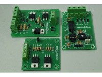
Hardware:
The concept consists of two versions of hardware, first one is the basic concept and can be used with a low voltage (LV AC) supply (tested with 40VAC, here an external rectifier bridge must be used). The other hardware version can be used as a more practical circuit with high voltage (HV AC, 230V mains AC). The HV version (160515-2 v1.1) is tested with two 100W lightbulbs. For higher loads diodes D5 to D8 (the local bridge rectifier) would have to be replaced with a higher rating, but is not advisable. The MOSFETs then need a heat sink each and larger diodes would have to be used. The layout is not really designed for this. Both circuits are educational and therefore experimental.
LV AC – Two-anode MOSFET thyristor
K1: Gate signal input + ground
K2: Load 1 (A1), Load2 (A2) output and pulsating DC +V input (LV external bridge rectifier needed!)
HV AC - Two-anode MOSFET thyristor
K1: Load 1 (A1), Load2 (A2) output and +HV output
K2: Gate signal input + ground
K3: Mains AC input
Circuit Description LV AC - Two-anode MOSFET thyristor 160515-1 v1.1:
This simple circuit is used to explain the concept of hardware where two anodes are formed by N-channel MOSFETs T1 and T2. Load can be connected from +V to drain of each MOSFET so that two loads can be connected (see wiring diagram). For testing, Load 1 =150 Ω 10W and 1 =150 Ω 10W load resistors were used for testing. SCR TH1 drives the MOSFET T1. For MOSFET T2, gate pulses are obtained from the drain of T1. SCR TH1 is used to control the voltage across the loads connected from the anodes to +V by using mains synchronized gate pulses. We designed a simple circuit for this purpose which also includes an extra full wave rectifier needed with this LV circuit. Look for project ‘SCR gate pulse generator [180611]’. The LV circuit is tested at 40 VAC. An external bridge rectifier is needed (on 180611) without capacitor for +V supply. The full wave rectified output +HV on 180611 (K1) is connected to +V of K2 and GND of K1. The moment of the rising edge of the gate pulse applied at K1 in relation to the zero crossing of the mains voltage controls the voltage across the load.
The thyristor TH1 is of type P0102DA 1AA3 and has an industry standard pinout. So other thyristors in a TO-92 package will work as well. Be cautious for types with reverse pinout like a BT149G. Trigger current is low for these types, 200 µA max for the one used here. For protection an extra 10 kΩ resistor (R1) is placed in series with the gate. The single sided PCB (the pdf with topoverlay shows copper on bottom) is designed with room to spare between components (55 x 55 mm) and all components can be mounted and soldered in a matter of minutes. The layout has a copper plane connected to ground and is therefore not suitable for high voltages! Components costs should be less than 10 euro.
Circuit description HV AC - Two-anode MOSFET thyristor 160515-2 v1.1:
This circuit is meant for resistive loads such as incandescent lamps or other loads that are suitable to be controlled by a dimmer (100 W max.). The circuit consists of bridge rectifier D5..D8, SCR TH1, MOSFETS T1, T2 etc. The heart of the circuit is SCR TH1 used to control the two anodes formed by two N-channel MOSFETs T1 & T2. Two loads can be connected from +HV to drain of each MOSFET (A1 and A2). Mains AC voltage can be connected to connector K3. The output from the bridge rectifier is used as +HV for the circuit and is connected to the rest of the circuit by the loads through D3 and D4. Both loads can be connected at connector K1. Have a look at the wiring diagram. Like the LV circuit the gate pulse for TH1 is applied at connector K2. External circuit ‘SCR gate pulse generator [180611]’ is also used to produce the mains synchronized gate pulses. SCR TH1 drives the MOSFET T1. For MOSFET T2, gate pulses are obtained from the drain of T1. Resistors R4, R5 with diode D9 provide smooth switching of MOSFET T2. R2, R3 and R5 are 500 V resistors since depending on the pulse phase the maximum voltage across the resistors is almost the mains voltage. D9 and R4 are responsible for charge discharge of gate capacitor of T2 respectively. Zener diodes D1 and D2 are for protection of the gate of the MOSFETs T1 and T2 and limit the gate voltages to12V maximum. The trigger current of thyristor BT151-800R is 2 mA typical and 15 mA maximum. In theory this means the trigger current delivered by 180611 could be too low but not likely. It’s no problem to lower resistor R9 on 180611-1 v1.0 to 150 Ω. The circuit is tested with two loads of 100 W with input current of 0.43A and power factor of 1.0 (for resistive loads) in both the cases. The single sided PCB (the pdf with topoverlay shows copper on bottom) is designed with regards to safety rules for mains voltages. The screw terminals have a 7.5 mm lead spacing to assure a 3 mm clearance. Be aware that once the mains voltage is present on K3 all components are connected to the mains voltage. Also the pulse generator connected to K2 and its +5 V power supply! Component costs should be less than 25 euro.
External control 180611 for LV – Two-anode MOSFET thyristor 160515-1 v1.1:
The SCR TH1 controls the switching of MOSFET T1 which in turn controls the MOSFET T2. Here, the SCR phase angle is controlled by potentiometer P1 on SCR gate pulse generator 180611. The amount of power to Load 1 and Load 2 depends on the setting of potentiometer P1. When the potentiometer reaches to its extreme value either Load 1 or load 2 has maximum or minimum power.
External control 180611 for HV – Two-anode MOSFET thyristor 160515-2 v1.1:
The full wave rectifier +HV output frequency is 100 Hz. These 100Hz pulses are fed to the SCR TH1 when one or both loads are connected through D3 and D4. The SCR TH1 controls the switching of MOSFET T1 which in turn controls the MOSFET T2. Here, the SCR phase angle is controlled by potentiometer P1 on SCR gate pulse generator 180611. Power applied to Load 1 and Load 2 is controlled by varying the potentiometer P1. When the potentiometer reaches to its extreme value the voltage across either Load 1 or Load 2 is maximal or minimal.
Testing Procedure for Two-anode MOSFET thyristor
(look closely at the wiring diagram)
LV AC – Two-anode MOSFET thyristor
• Bridge rectifier is not included on the PCB and hence an external bridge rectifier (on 180611) needs to be used without filter capacitor for generating +V (pulsating DC). This +V (+HV of K1 on 180611) needs to be connected at connector K2. Also both grounds should be connected although they are already connected if R3 (0 Ω or jumper wire) on 180611 is mounted. Leave R3 on 180611 unmounted if the HV test circuit is also to be tested.
• Connect Load 1 and Load 2 at K2 with one end to +V and the other to A1 and A2.
• Load 1 and Load 2 are 150 Ω 10W resistors for each anode.
• Load 1 will be turned ON and Load 2 will be OFF.
• Connect the SCR gate pulse generator 180611 and supply 5V to the control board.
• Both power circuit ground (K1) and control circuit ground (K4 on 180611) must be connected to each other.
• Vary potentiometer P1 which controls the power of Load 1 and Load 2.
• Due to the power output to the resistors, they can heat up (at 40 VAC about 10 W each max) and hence precautions should be taken while handling.
HV AC – Two-anode MOSFET thyristor
• Connect Load 1 and Load 2 at K1 with one end to +HV and the other to A1 and A2.
• Load 1 and Load 2 are 100 W bulbs but 25 W will also do as a load for each anode.
• Connect AC mains supply to the connector K3 of the board.
• Load 1 will be turned ON and Load 2 will be OFF.
• Disconnect the mains, both terminals.
• Remove R3 on the SCR gate pulse generator (180611).
• Connect the control circuit to the power circuit as shown in the wiring diagram and supply 5V to the control board.
• Power circuit ground (K2) and control circuit ground (K4) must be connected.
• Connect the mains.
• Vary trimmer P1 on 180611 using a plastic adjustment tool (for instance H-90/H-91/H-92-1 from Bourns). P1 controls the power output to load 1 and Load 2 and thus light intensity. The light bulbs can also get hot!
If available use a variable auto transformer (the smallest ones are usually 500 VA) and a 230 VA 1:1 safety transformer to power the HV circuit. The latter is necessary since an autotransformer has one output directly connected to the input! Using an additional safety transformer you can then gradually and safely increase the mains voltage. But never go to 100 %. The output voltage at 100 % is often 15 % higher than the input voltage or even more at light loads. Nice to test overvoltage conditions (without the safety transformer of course) but not advisable here.
Also see
https://www.elektormagazine.com/labs/scr-gate-pulse-generator-180611-1
Literature:
Shustov M.A. Analogues of thyristors with field effect transistors // Radio (Russia). 2016. No. 12. P. 27.
Bill of material 160515-1 v1.1:
Resistor
R1,R5, R8 = 10 kΩ, 5%, 0.25W, 250V
R2 = 15 k, 5%, 0.25W, 250V
R3 = 5.6 k, 5%, 0.25W, 250V
R4, R7 = 100 Ω, 5%, 0.25W, 250V
R6 = 22 kΩ, 5%, 0.25W, 250V
Semiconductor
D1, D2 = 1N5242BTR - Zener, 12 V, 5 %, 0.5 W DO-35
TH1 = P0102DA 1AA3 - SCR THYRISTOR, 800mA, 400V, TO-92
T1, T2 = SPP15N60C3XKSA1 N-channel MOSFET, 600 V, 15A, TO-220
Other
K1 = Terminal block 5.08 mm, 3-way, 630 V
K2 = Terminal block 5.08 mm, 3-way, 630 V
Misc.
PCB 160515-1 v1.1
Bill of material 160515-2 v1.1:
Resistor
R1 = 100 kΩ, 5%, 0.25W, 250V
R2, R3 = 470 kΩ, 5%, 1 W, 500V
R4 = 10 kΩ, 5%, 0.25W, 250V
R5 = 330 kΩ, 5 %, 1 W, 500 V
Semiconductor
D1, D2 = 1N4742A - zener, 12V, 5 %, 1 W, DO-41
D3-D9 = 1N4007, DO-41
TH1 = BT151-800R, thyristor, 800 V, 7.5 A, Igt 15 mA max., TO-220
T1, T2 = SPP15N60C3XKSA1 N-channel MOSFET, TO-220
Other
K1 = Terminal block 7.68 mm, 3-way, 630 V
K2,K3 = Terminal block 7.68 mm, 2-way, 630 V
Misc.
PCB 160515-2 v
Thyristor (triac) load switches, due to their unavoidable design features are characterized by high cathode-anode voltage drop on them in the open state as well as by low switching performance. Due to this, a remarkable power dissipates on such switching elements, sometimes leading to overheating and failure of the semiconductor device. At the same time, the useless heating of the semiconductor device consumes electric power, which, under conditions of mass industrial and household use of thyristors and triacs, leads to large-scale losses.
The Two-anode thyristor controlled load switch (Two-anode MOSFET thyristor). The circuit has input characteristics of a high-speed thyristor, but the losses on its open switching elements are almost two orders of magnitude lower than for conventional thyristors. In addition, the proposed load switch has, in contrast to the conventional thyristors, two outputs. First output is in the switched-on state and the second output is in the switched-off state. These outputs are switched over according to the thyristor switching.
When using a Two-anode MOSFET thyristor in an alternating current network with a power controller in the circuit of one of its channels, the unused sine wave sections in case of classical thyristors will not be lost and can be used in the circuit of its second load channel.
The use of MOSFET transistors in the proposed version of a two-anode thyristor provides its higher switching performance, extremely low losses and high input resistance. These features and parameters of the two-anode MOSFET thyristor allow it to be approximately an ideal switching element.
Hardware:
The concept consists of two versions of hardware, first one is the basic concept and can be used with a low voltage (LV AC) supply (tested with 40VAC, here an external rectifier bridge must be used). The other hardware version can be used as a more practical circuit with high voltage (HV AC, 230V mains AC). The HV version (160515-2 v1.1) is tested with two 100W lightbulbs. For higher loads diodes D5 to D8 (the local bridge rectifier) would have to be replaced with a higher rating, but is not advisable. The MOSFETs then need a heat sink each and larger diodes would have to be used. The layout is not really designed for this. Both circuits are educational and therefore experimental.
LV AC – Two-anode MOSFET thyristor
K1: Gate signal input + ground
K2: Load 1 (A1), Load2 (A2) output and pulsating DC +V input (LV external bridge rectifier needed!)
HV AC - Two-anode MOSFET thyristor
K1: Load 1 (A1), Load2 (A2) output and +HV output
K2: Gate signal input + ground
K3: Mains AC input
Circuit Description LV AC - Two-anode MOSFET thyristor 160515-1 v1.1:
This simple circuit is used to explain the concept of hardware where two anodes are formed by N-channel MOSFETs T1 and T2. Load can be connected from +V to drain of each MOSFET so that two loads can be connected (see wiring diagram). For testing, Load 1 =150 Ω 10W and 1 =150 Ω 10W load resistors were used for testing. SCR TH1 drives the MOSFET T1. For MOSFET T2, gate pulses are obtained from the drain of T1. SCR TH1 is used to control the voltage across the loads connected from the anodes to +V by using mains synchronized gate pulses. We designed a simple circuit for this purpose which also includes an extra full wave rectifier needed with this LV circuit. Look for project ‘SCR gate pulse generator [180611]’. The LV circuit is tested at 40 VAC. An external bridge rectifier is needed (on 180611) without capacitor for +V supply. The full wave rectified output +HV on 180611 (K1) is connected to +V of K2 and GND of K1. The moment of the rising edge of the gate pulse applied at K1 in relation to the zero crossing of the mains voltage controls the voltage across the load.
The thyristor TH1 is of type P0102DA 1AA3 and has an industry standard pinout. So other thyristors in a TO-92 package will work as well. Be cautious for types with reverse pinout like a BT149G. Trigger current is low for these types, 200 µA max for the one used here. For protection an extra 10 kΩ resistor (R1) is placed in series with the gate. The single sided PCB (the pdf with topoverlay shows copper on bottom) is designed with room to spare between components (55 x 55 mm) and all components can be mounted and soldered in a matter of minutes. The layout has a copper plane connected to ground and is therefore not suitable for high voltages! Components costs should be less than 10 euro.
Circuit description HV AC - Two-anode MOSFET thyristor 160515-2 v1.1:
This circuit is meant for resistive loads such as incandescent lamps or other loads that are suitable to be controlled by a dimmer (100 W max.). The circuit consists of bridge rectifier D5..D8, SCR TH1, MOSFETS T1, T2 etc. The heart of the circuit is SCR TH1 used to control the two anodes formed by two N-channel MOSFETs T1 & T2. Two loads can be connected from +HV to drain of each MOSFET (A1 and A2). Mains AC voltage can be connected to connector K3. The output from the bridge rectifier is used as +HV for the circuit and is connected to the rest of the circuit by the loads through D3 and D4. Both loads can be connected at connector K1. Have a look at the wiring diagram. Like the LV circuit the gate pulse for TH1 is applied at connector K2. External circuit ‘SCR gate pulse generator [180611]’ is also used to produce the mains synchronized gate pulses. SCR TH1 drives the MOSFET T1. For MOSFET T2, gate pulses are obtained from the drain of T1. Resistors R4, R5 with diode D9 provide smooth switching of MOSFET T2. R2, R3 and R5 are 500 V resistors since depending on the pulse phase the maximum voltage across the resistors is almost the mains voltage. D9 and R4 are responsible for charge discharge of gate capacitor of T2 respectively. Zener diodes D1 and D2 are for protection of the gate of the MOSFETs T1 and T2 and limit the gate voltages to12V maximum. The trigger current of thyristor BT151-800R is 2 mA typical and 15 mA maximum. In theory this means the trigger current delivered by 180611 could be too low but not likely. It’s no problem to lower resistor R9 on 180611-1 v1.0 to 150 Ω. The circuit is tested with two loads of 100 W with input current of 0.43A and power factor of 1.0 (for resistive loads) in both the cases. The single sided PCB (the pdf with topoverlay shows copper on bottom) is designed with regards to safety rules for mains voltages. The screw terminals have a 7.5 mm lead spacing to assure a 3 mm clearance. Be aware that once the mains voltage is present on K3 all components are connected to the mains voltage. Also the pulse generator connected to K2 and its +5 V power supply! Component costs should be less than 25 euro.
External control 180611 for LV – Two-anode MOSFET thyristor 160515-1 v1.1:
The SCR TH1 controls the switching of MOSFET T1 which in turn controls the MOSFET T2. Here, the SCR phase angle is controlled by potentiometer P1 on SCR gate pulse generator 180611. The amount of power to Load 1 and Load 2 depends on the setting of potentiometer P1. When the potentiometer reaches to its extreme value either Load 1 or load 2 has maximum or minimum power.
External control 180611 for HV – Two-anode MOSFET thyristor 160515-2 v1.1:
The full wave rectifier +HV output frequency is 100 Hz. These 100Hz pulses are fed to the SCR TH1 when one or both loads are connected through D3 and D4. The SCR TH1 controls the switching of MOSFET T1 which in turn controls the MOSFET T2. Here, the SCR phase angle is controlled by potentiometer P1 on SCR gate pulse generator 180611. Power applied to Load 1 and Load 2 is controlled by varying the potentiometer P1. When the potentiometer reaches to its extreme value the voltage across either Load 1 or Load 2 is maximal or minimal.
Testing Procedure for Two-anode MOSFET thyristor
(look closely at the wiring diagram)
LV AC – Two-anode MOSFET thyristor
• Bridge rectifier is not included on the PCB and hence an external bridge rectifier (on 180611) needs to be used without filter capacitor for generating +V (pulsating DC). This +V (+HV of K1 on 180611) needs to be connected at connector K2. Also both grounds should be connected although they are already connected if R3 (0 Ω or jumper wire) on 180611 is mounted. Leave R3 on 180611 unmounted if the HV test circuit is also to be tested.
• Connect Load 1 and Load 2 at K2 with one end to +V and the other to A1 and A2.
• Load 1 and Load 2 are 150 Ω 10W resistors for each anode.
• Load 1 will be turned ON and Load 2 will be OFF.
• Connect the SCR gate pulse generator 180611 and supply 5V to the control board.
• Both power circuit ground (K1) and control circuit ground (K4 on 180611) must be connected to each other.
• Vary potentiometer P1 which controls the power of Load 1 and Load 2.
• Due to the power output to the resistors, they can heat up (at 40 VAC about 10 W each max) and hence precautions should be taken while handling.
HV AC – Two-anode MOSFET thyristor
• Connect Load 1 and Load 2 at K1 with one end to +HV and the other to A1 and A2.
• Load 1 and Load 2 are 100 W bulbs but 25 W will also do as a load for each anode.
• Connect AC mains supply to the connector K3 of the board.
• Load 1 will be turned ON and Load 2 will be OFF.
• Disconnect the mains, both terminals.
• Remove R3 on the SCR gate pulse generator (180611).
• Connect the control circuit to the power circuit as shown in the wiring diagram and supply 5V to the control board.
• Power circuit ground (K2) and control circuit ground (K4) must be connected.
• Connect the mains.
• Vary trimmer P1 on 180611 using a plastic adjustment tool (for instance H-90/H-91/H-92-1 from Bourns). P1 controls the power output to load 1 and Load 2 and thus light intensity. The light bulbs can also get hot!
If available use a variable auto transformer (the smallest ones are usually 500 VA) and a 230 VA 1:1 safety transformer to power the HV circuit. The latter is necessary since an autotransformer has one output directly connected to the input! Using an additional safety transformer you can then gradually and safely increase the mains voltage. But never go to 100 %. The output voltage at 100 % is often 15 % higher than the input voltage or even more at light loads. Nice to test overvoltage conditions (without the safety transformer of course) but not advisable here.
Also see
https://www.elektormagazine.com/labs/scr-gate-pulse-generator-180611-1
Literature:
Shustov M.A. Analogues of thyristors with field effect transistors // Radio (Russia). 2016. No. 12. P. 27.
Bill of material 160515-1 v1.1:
Resistor
R1,R5, R8 = 10 kΩ, 5%, 0.25W, 250V
R2 = 15 k, 5%, 0.25W, 250V
R3 = 5.6 k, 5%, 0.25W, 250V
R4, R7 = 100 Ω, 5%, 0.25W, 250V
R6 = 22 kΩ, 5%, 0.25W, 250V
Semiconductor
D1, D2 = 1N5242BTR - Zener, 12 V, 5 %, 0.5 W DO-35
TH1 = P0102DA 1AA3 - SCR THYRISTOR, 800mA, 400V, TO-92
T1, T2 = SPP15N60C3XKSA1 N-channel MOSFET, 600 V, 15A, TO-220
Other
K1 = Terminal block 5.08 mm, 3-way, 630 V
K2 = Terminal block 5.08 mm, 3-way, 630 V
Misc.
PCB 160515-1 v1.1
Bill of material 160515-2 v1.1:
Resistor
R1 = 100 kΩ, 5%, 0.25W, 250V
R2, R3 = 470 kΩ, 5%, 1 W, 500V
R4 = 10 kΩ, 5%, 0.25W, 250V
R5 = 330 kΩ, 5 %, 1 W, 500 V
Semiconductor
D1, D2 = 1N4742A - zener, 12V, 5 %, 1 W, DO-41
D3-D9 = 1N4007, DO-41
TH1 = BT151-800R, thyristor, 800 V, 7.5 A, Igt 15 mA max., TO-220
T1, T2 = SPP15N60C3XKSA1 N-channel MOSFET, TO-220
Other
K1 = Terminal block 7.68 mm, 3-way, 630 V
K2,K3 = Terminal block 7.68 mm, 2-way, 630 V
Misc.
PCB 160515-2 v
Diskussion (0 Kommentare)