
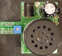
T-Board Audio Amplifier [150002-1]
Up until now we only had digital T-Boards. Why not an analog one? We asked ourselves what could be a useful circuit when experimenting with an analog design. First thought was audio. How about a little amplifier and speaker so no extra cables or 3,5 mm jacks need to be connected. Also no extra speaker has to be connected, all you need is just on one little PCB.
Up until now we only had digital T-Boards. Why not an analog one? We asked ourselves what could be a useful circuit when experimenting with an analog design. First thought was audio. How about a little amplifier and speaker so no extra cables or 3,5 mm jacks need to be connected. Also no extra speaker has to be connected, all you need is just on one little PCB. Of course an AC adapter or battery is necessary as a power supply. The idea was to design the PCB with a small protrusive part with 2 headers for the audio input signal and an alternative power supply for the T-Board. But to be honest it’s not really a T anymore, or is it?
Originally the title was T-Board LM386 amplifier. But what is the point of using an integrated circuit that can also be placed on a bread-board directly. We want to keep the PCB as small as possible so the logical choice is the use of SMDs. First we need to determine how much power is needed for little PCB mounted enclosed speakers. Apparently 0.15 W is a common value with a maximum of 0.2 W or there about. Many analog amplifiers still have a lot of passive components, so we looked for modern class-D amplifiers. The small power ones for use in single supply applications almost all have bridge outputs. That way no large coupling capacitors have to be used. But we also would like the circuit to be used with an external speaker if better quality is required. Don’t expect too much from these little PCB speakers. They have resonant peaks and very high low-frequency roll-off. 500 Hz or more is not uncommon. This means that frequencies below the range of the speaker should not be applied to it. This would produce strong audible distortion because the membrane/driver would go beyond its maximum permissible physical excursion and this can also cause permanent damage. So a coupling capacitor is still needed. An external speaker is directly connected to the Class-D amplifier outputs. A jumper in series with the PCB speaker is added to disable it.
The power supply range of the SSM2305 (IC2) from Analog Devices is 2.5 V to 5.5 V. At 2.5 V it delivers a little over 0.3 W undistorted into an 8 Ω load. This is more than enough for our purpose. To minimize HF radiation from the switching outputs ferrite beads and small capacitors (L1/L2/C8/C9) are used to filter the outputs for the speakers. The shutdown control is not used and IC1 is permanently enabled by R6, by connecting pin1 to the power supply. For most applications the fully differential input is not suitable and a single ended input is more fitting. A single ended solution is possible without IC1. One of the input capacitors C4 or C5 can be connected to ground leaving the other one as input. We used an inverter to make a differential signal from the input of the PCB. Sensitivity is higher and the inputs of IC2 are better protected from extreme input signals. In principle coupling capacitors C4 and C5 are not needed since the DC level of both opamps of IC1 are at half the supply voltage. However the datasheet states that leaving them out can increase output offset and degrade the DC PSRR performance. The low frequency roll-off caused by C4/C5 is about 20 Hz. So external speaker get the full audio spectrum. IC1 (TSV912AIYST) is a fast (8 MHz) dual rail-to-rail input/output opamp and can also work with a power supply voltage of 2.5 to 5.5 V. It has a low quiescent current (0,78 mA per opamp at 2.5 V) and low input bias current (10 pA max. at 25 °C). The latter causes no extra offset in the resistors of the inverter. The relatively high value of input coupling capacitor C1 makes a very low roll-off (1.6 Hz) and has virtually no influence. To protect the input amplifier, D1 clips any high input voltage through R1 to just outside the power supply rail. The high sensitivity (100 mV for maximum undistorted power into an 8 Ω load) makes a potentiometer (P1) at the input necessary. The input impedance varies, depending on level set by P1, between 9.1 and 10 kΩ. We’re not going into distortion figures, the applications (mainly testing) of this project and the audio quality of the speaker makes it not that interesting. The slider of P1 is also connected to header K1. Who knows, maybe it can be put to use in some applications.
As a power regulator a linear one is simply not an option. This amplifier should work with most AC adapters, so maximum input voltage must be possible as high as 12 V or more. The power loss in a linear regulator would simply be impractical then. The only alternative (except for batteries) is a simple step-down DC-DC-regulator. The choice was made for another Analog Devices IC, the ADP2300A (IC3). The ADP2300A (700 kHz) is preferred over the ADP2301 (1.4 MHz) because of its slightly higher efficiency. Its only available in a 6-lead TSOT (Thin Small Outline Transistor Package, also called UJ-6) but can handle 1.2 A maximum load current. There are few components necessary to make the circuit complete. Almost all are passive except for 1 diode (power input polarity protection diode D3 not counted). The circuit with the ADP2300A is made according to the standard application. Inductor L4 is chosen for the lower input voltage range. The formula in the datasheet to calculate the inductor with a ripple current of 30 % of the maximum load current gives a value of 10 to 12 µH for 5 Vin (depends on the exact drop voltage of (D2) and the exact maximum current). This is rounded to a standard value of 10 µH. With higher voltages the ripple current will be higher. According to the formula the inductor would have to be in the range of 23 to26 µH when the input voltage is 20 V. The maximum undistorted voltage with an 4 Ω load is roughly 3.6 Vpeak-peak, giving a maximum peak supply current of about 0.45 A. IC3 has an enable input we use to set the minimum startup voltage. We chose 3.6 V. With the diode drop of D3 it will take about 3.8 V or 3.9 V to startup the DC-DC-regulator. We tried lower levels since the output voltage can be 0,85 x the input voltage. 3 V at Vin should be able to produce a stable 2.5 V. But at these low levels with a speaker connected and signal applied a kind of hiccups occurred and the input voltage must be higher before switching on properly. So we set the minimum voltage higher. The input polarity protection diode D3 is partly also the cause of this. With virtually no current the voltage drop of D3 is very low. When the regulator and Class-D amplifier are turned on, the voltage drop of D3 increases and the voltage at Vin of IC3 is lower again. Voltage divider R9/R10 could have been connected to the anode of D3 , but what happens to IC3 with wrong polarity applied?
The supply current of IC2 is a rectified sine and will be small at times, and because of this the average efficiency of the DC-DC-regulator will be smaller. Some measurements from our prototypes:
Table 1
------------4.3 Vpp/8 Ω (equals 289 mW)---------------- ---------4.3 Vpp/8 Ω + 100 µH-----
Vin [V] Iin [mA] Pin [mW] η [%] Iin [mA] Pin [mW] η [%]
4 126 504 57.3 111 444 65.1
5 99 495 58.4 88 440 65.7
6 83 498 58 73.6 441.6 65.4
9 56 504 57.3 50.2 451.8 64
12 43 516 56 38.7 464.4 62.2
15 35 525 55 32 480 60.2
18 30 540 53.5 27.6 496.8 58.2
20 27.5 550 52.5 25.3 506 57.1
Table 2
------------3.6 Vpp/4 Ω (equals 405 mW)---------------- ---------3.6 Vpp/4 Ω + 100 µH-----
Vin [V] Iin [mA] Pin [mW] η [%] Iin [mA] Pin [mW] η [%]
4 222 888 45.6 178 (4.3 V) 765.4 52.9
5 168 840 48.2 148.4 742 54.6
6 137 822 49.3 121.5 729 55.6
9 91 819 49.5 80.9 728.1 55.6
12 69 828 48.9 61.6 739.2 54.8
15 56 840 48.2 50.3 754.5 53.7
18 47.7 858 47.2 42.8 770.4 52.6
20 43.3 866 46.8 39.06 781.2 51.8
We measured efficiency with a pure resistive load and the rough simulation of our speaker by placing 100 µH in series with the load resistor. Efficiency is increased by the induction of the speaker. High frequency currents are suppressed. The average switching frequency of the SSM2305A is 280 kHz. From table 1 we see that the lowest efficiency is at 20 V with 52.5 % for a resistive load and 57.1 % for the speaker, as was to be expected. Highest efficiency is at 5 V for both, 58.4 % for the resistive load and 65.7 % for the speaker. At 4 V the gain in efficiency with a speaker is almost 8 % and less than 5 % at 20 V. The maximum efficiency at 5 V was not a design requirement. Let’s call it a strange coincidence.
From table 2 we can clearly see that overall efficiency is lower if a 4 Ω speaker is used. The higher currents and voltage drops have a strong effect with a power supply voltage this low. To give an idea, without D3 at 4 V efficiency is 49 %. The lowest power supply voltage for a 4 Ω load with maximum power applied is 4.5 V. A lower supply voltage can cause hiccups.
Some other measurements:
Quiescent current (no signal) 7.5 mA (4 V)
2.3 mA (20 V)
Max. sensitivity (P1 max.) 100 mV (1 kHz/289 mW/8 Ω)
85 mV (1 kHz/405 mW/4 Ω)
Led current 1.67 mA
Supply Voltage 4…20 V (8 Ω)
4.5…20 V (4 Ω)
To filter the ripple of the power supply and other HF interferences a common mode choke (L3) is placed between the DC-DC-regulator and the Class-D amplifier. We used the DC barrel jack K3 to switch off the ground connection to the power supply connection of K2. This is done to prevent an earth loop if the voltage of K3 would be used to power the circuit on the bread board and the T-Board. Connecting ‘0’ of K2 and GND of K1 short-circuits part of common mode choke L3 and will degrade performance of the T-Board. We strongly recommend using a separate power supply for the T-Board, preferably through K3.
The PCB is double sided in both layout and mounted components. All through hole components are located on the top side accept for the headers K1 and K2. These headers with small rounded pins are placed on the bottom side so the PCB can easily be placed on a bread board (the whole point of our T-Board series). All SMDs are mounted on the bottom side. The SSM2305 is also available in a 3 mm × 3 mm lead frame chip scale package (LFCSP). But the lower thermal resistance (junction to ambient 62 instead of 210 for the 8-lead MSOP we used) is not required with this low power supply voltage.
The coupling capacitor in series with the speaker looks kind of big but it’s cheap and the rated ripple current of 240 mA should be higher than the maximum (undistorted) current through the speaker, which is less than 200 mA. The 100 V version of the bipolar electrolytic capacitor series qualified.
The footprint for P1 is designed to handle 3 different pinouts from the series from Vishay Sfernice, so even types from other manufacturers should fit (in case you want to build it yourself. The SMD’s used are not that difficult to solder…
Bill of materials PCB 150002-1 v1.1
Resistor
R1 = 1 kΩ, 0W1, 1 %, SMD 0603
R2-R6 = 100 kΩ, 0W1, 1 %, SMD 0603
R7 = 22 kΩ, 0W1, 1 %, SMD 0603
R8,R10 = 10 kΩ, 0W1, 1 %, SMD 0603
R9 = 20 kΩ, 0W1, 1 %, SMD 0603
R11 = 390 Ω, 0W1, 1 %, SMD 0603
P1 = 10 kΩ, 0W5, 10 %, trimmer (Vishay Sfernice T73YU103KT20)
Capacitor
C1,C2 = 1 µF, 25 V, 10 %, X7R, SMD 0805
C3,C6,C11,C12,C14 = 100 nF, 16 V, 10 %, X7R, SMD 0603
C4,C5 = 220 nF, 10 V, 10 %, X7R, SMD 0603
C7 = 10 µF, 6V3, 20 %, X5R, SMD 0603
C8,C9 = 1 nF, 50 V, 5 %, C0G/NP0, SMD 0603
C10 = 47 µF, 100 V, 20 %, diam. 13 mm, lead spacing 5 mm, Ir 240 mA
C13 = 22 µF, 6V3, 10 %, X5R, SMD 1206
C15 = 10 µF, 25V, 10 %, X5R, SMD 1206
Inductor
L1,L2 = BLM18KG601SN1D, 1.3A, 0.15Ω, 600Ω@100MHz, Murata, SMD 0603
L3 = ACM4520-231-2P-T, SMD Common Mode Choke 3 A, 2x50mΩ, 230Ω@100MHz
L4 = 10 µH, 2.1 A, shielded, SMD (Laird TYS5040100M-10)
Semiconductor
D1 = PESD5Z2.5, SMD SOD-523
D2,D3 = PMEG6030EP, SMD SOD-128
D4 = led, green, T-1 3 mm, through hole, low current
IC1 = TSV912AIYST, SMD MSOP-8
IC2 = SSM2305RMZ-REEL7, SMD RM-8
IC3 = ADP2300AUJZ-R7, SMD UJ-6
Other
K1,K2 = header, through hole (4-way) pitch 2.54 mm
K3 = DC barrel jack, 1.95 mm pin, 12 V, 3 A
PC1,PC2 = Terminal pin, 1.3 mm diam.
JP1 = 2-way pinheader SIL, 2.54 mm spacing, vertical
JP1 = Single shunt jumper 2.54 mm spacing
LS1 = PCB enclosed speaker, diam. 31.9 mm, lead spacing 17.53 mm (RS-online 7243119)
Misc.
PCB 150002-1 v1.1
Alternative 1 for LS1: MCABS-201-RC Multicomp (Farnell 2361100)
Alternative 2 for LS1: 2823 (K 23 PC - 8 Ohm) Visaton (Farnell 2357167)
Diskussion (0 Kommentare)