
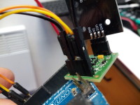
SPI to WS2812B converter
3 ways to make SPI compatible with WS2812B-type addressable RGB LEDs.
For the WS2812B-type addressable RGB LED (also known as 'NeoPixel') a logic ‘0’ is expected to be a pulse of 400 ns followed by an 800 ns space. A logic ‘1’ is encoded as an 800 ns pulse followed by a 450 ns space. However, according to the datasheet, all these durations have a tolerance of ±150 ns. So, for a logic ‘0’, a pulse of 300 instead of 400 ns followed by a space of 700 instead 800 ns is fine too, and a logic ‘1’ is allowed to be a 700 ns pulse followed by a 300 ns space. With these values the data rate becomes 1 MHz, perfect for SPI.
At 1 MHz the SPI SCK signal is a square wave consisting of 500 ns pulses and 500 ns spaces. To turn it into a WS2812B-compatible signal we must shorten the pulses for logic ‘0’s and make the pulses for logic ‘1’s a bit longer.
The data is found in the SPI’s MOSI signal.
This circuit works in SPI modes 0, 1 and 3.
Notes:
Like the first circuit, this one also works in SPI modes 0, 1 and 3.
You can decrease the current consumption of this circuit by replacing R3 by a P-type MOSFET with its gate connected to the gate of T3. Now when the circuit is idle the output stage is disconnected from the power supply and no current can flow.
You could do something similar with monostable multivibrators.
Fun fact: you can turn the output signal of these circuits back into SPI with a single monostable multivibrator that triggers on the rising edges of the signal. If it produces 500 ns pulses for each rising edge, then the result is the SCK signal. At the falling edge of these pulses the data is stable low or high. This is equal to a SPI signal in mode 1.
At 1 MHz the SPI SCK signal is a square wave consisting of 500 ns pulses and 500 ns spaces. To turn it into a WS2812B-compatible signal we must shorten the pulses for logic ‘0’s and make the pulses for logic ‘1’s a bit longer.
The data is found in the SPI’s MOSI signal.
Circuit 1
If we extract the rising edges of the SCK signal, then we must turn them into 300-ns pulses when MOSI is low and 700 ns pulses when MOSI is high. For the schematic, see the KiCad project 220020-1 in the download section. It is easy to turn a rising edge into a 300 ns pulse with a differentiator. If we AND the SCK and MOSI signals together, we obtain a signal with 500 ns pulses when MOSI is high. If we now OR the 300 and 500 ns pulses together, we get a signal with different pulse lengths for zeroes and ones. We can make these pulses a bit longer by adding an integrator. This will make the zero pulses longer too, but we can compensate for that by adjusting the differentiator. A MOSFET buffers the signal. A second MOSFET inverts the signal back to normal. A third transistor lets you disable the circuit’s output, so the LEDs won’t listen to data that is not intended for them.This circuit works in SPI modes 0, 1 and 3.
Notes:
- It is highly recommended to disable interrupts when data is transmitted to the LEDs.
- Use a good, capable power supply for the LEDs .
- The value of the supply voltage of the SPI converter must be the same as that of the LED strip.
Circuit 1 Simplified
The second circuit (KiCad project 220020-2) uses MOSI to control the pulse length of SCK. When MOSI is low, C1 and R1 form a differentiator that shortens the SCK pulses. When MOSI is high, R1 is disconnected and C1 simply passes the SCK pulses to T2. When SCK is high, T2 conducts and C2 is discharged. When SCK goes low, T2 stops conducting and C2 is charged by R2, effectively delaying the falling edge of SCK. Now the SCK pulses are longer. T3 buffers and inverts the signal.Like the first circuit, this one also works in SPI modes 0, 1 and 3.
You can decrease the current consumption of this circuit by replacing R3 by a P-type MOSFET with its gate connected to the gate of T3. Now when the circuit is idle the output stage is disconnected from the power supply and no current can flow.
Now With Schmitt-Triggers
The third circuit (KiCad project 220020-3) is based on Schmitt trigger NAND gates. This looks even simpler but there are, of course, way more transistors involved. Now the pulses for the zeroes and the ones are created independently from each other. SCK provide the zeroes and MOSI the ones. The gate on the right merges them into one signal. This circuit only works in SPI modes 1 and 2.You could do something similar with monostable multivibrators.
Fun fact: you can turn the output signal of these circuits back into SPI with a single monostable multivibrator that triggers on the rising edges of the signal. If it produces 500 ns pulses for each rising edge, then the result is the SCK signal. At the falling edge of these pulses the data is stable low or high. This is equal to a SPI signal in mode 1.
Diskussion (0 Kommentare)