

LCR Meter Revisited (AU2019)
More than 7 years ago, Elektor published my 500 ppm LCR Meter AU2013. Since then I have developed a new LCR Meter, sacrificing a little on extreme accuracy for the sake of extended functionality.
A kit for the Elektor 50 Hz - 2 MHz LCR Meter is available here.
The new LCR Meter features:
Particular attention has been paid to its ease of implementation (calibration) and use (a rotary encoder is used to navigate through the menu and to change the frequency).
Overview
The power supply is done through a Mini-USB connector: use of a smartphone charger, an external battery (for smartphone) or connection to a computer (this last connection will also allow Firmware update).
It is also possible, but not recommended, not to use the integrated user interface, but to use only a suitable PC program.
Main Board
Circuits U66 and U67 allow synchronization with the sinusoidal signal of the voltage and current measurements of the DUT.
A jumper on connector J16 informs the Bootloader of an unconditional firmware update request.
The push button K1 (RESET) is optional (it is only used during the development phase).
USB Controller and Power Supplies (Figure 7 and 8)
An FT232RL (U2) circuit from FTDI serves as a USB/UART interface to the MCU. Normal power is supplied through the USB connector (J1), although it is possible to supply power through the J2 connector by putting a jumper between 1 and 2 of J3 instead of 2 and 3.
Four voltages are required to supply all circuits:
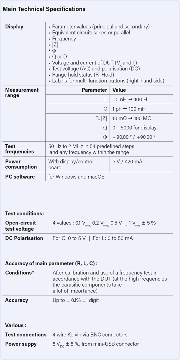
Only with your support The specifications of the LCR Meter are summarised in the below table. Before we start production of a kit, Elektor has launched a support campaign to gauge interest. If you would like to get your hands on a kit you can register, without making any formal commitment, online. The production of the kit will be started as soon as we have registered
The new LCR Meter features:
- Test frequency from 50Hz to 2MHz.
- 4 possible test voltages (100mV, 200mV, 500mV and 1V rms).
- Additional DC polarization up to 5V for capacitors and 50mA for inductors.
Particular attention has been paid to its ease of implementation (calibration) and use (a rotary encoder is used to navigate through the menu and to change the frequency).
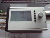
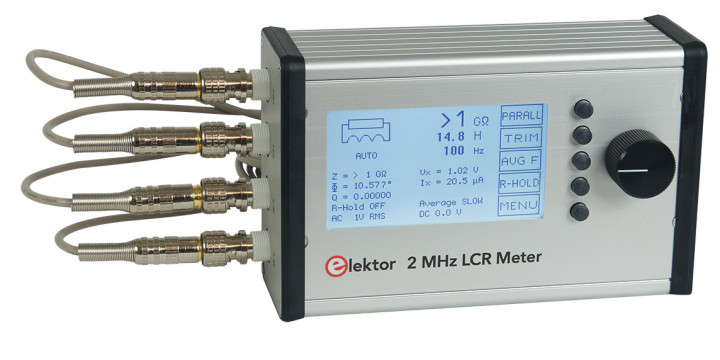
LCR Meter AU2019
Overview
The impedance (Z) is an important parameter to characterize passive electronic components (resistance, capacitor, inductance). It is a complex number which can be represented by a real part (R) and an imaginary part (X) such that Z = R + jX, or in polar form by the modulus of its impedance and the phase shift between voltage and current: Z.
To determine an impedance it is therefore necessary to measure at least two values (in magnitude and in phase), generally the voltage at the terminals of the component and the current flowing through it. The LCR Meter AU2019 uses the self-balanced bridge method with the use of a simple operational amplifier for the current/voltage converter (I-V converter, see Figure 1).
This simple method provides good measurement accuracy at a reasonable cost. Its main disadvantage is a frequency range limited in the high frequencies by the performance of the operational amplifier used.
To obtain a wide impedance measurement range (a few tens from mΩ to more than 100 MΩ) it is necessary to switch the precision resistor (R) used in the I-V converter. Unfortunately, common analog integrated switches (such as 74HC4052) introduce parasitic elements (mainly capacitors) which also limit the performance at high frequencies. This is why most similar instruments have a high frequency limited to 100 (see 200) kHz.
It is however possible, by an original design and the choice of high-performance components, to push the high frequency to 2 MHz without an exaggerated increase in cost, and while keeping the simplicity of realization.
The chosen solution is not to switch the 4 measuring resistors (thus reducing parasitic capacitance to a minimum) but to have four Amplifier + Resistor pairs, each selected according to the impedance to be measured.
The operational amplifiers used (AD8099 from Analog Devices) have a cut-off frequency of approx. 200 MHz at an output voltage of 2 V p-p and have the necessary muting control. The switches are PhotoMOS manufactured by Panasonic with a very low product (ON resistance x output capacitance).
Another important point is the choice of the method of generating the test frequency. It is easy and inexpensive today to use Direct Frequency Synthesis (DDS) components, with the advantage that any frequency in the 50 Hz / 2 MHz range can be generated. It is, moreover, easy to generate for the synchronous detector a signal of the same frequency, but with variable relative phase, thanks to a second DDS circuit synchronized to the first.
The user interface is reduced to a strict minimum:
- 240 x 128 pixel LCD graphic display.
- 5 push buttons.
- A rotary encoder with auxiliary contact.
The power supply is done through a Mini-USB connector: use of a smartphone charger, an external battery (for smartphone) or connection to a computer (this last connection will also allow Firmware update).
It is also possible, but not recommended, not to use the integrated user interface, but to use only a suitable PC program.
Main Board
Input Circuit (Figure 2)
The measurement is carried out with a 5-connection configuration [1] to minimize the influence of the measuring cables. Connectors J4 (High Drive) and J7 (Low Drive) supply power to the DUT (Device Under Test), while connectors J5 (High Sense) and J6 (Low Sense) allow the voltage to be measured as close as possible to the DUT. If a bias voltage is applied, the positive appears at J4/J5.
The PhotoMOS relays U54 to U57, which allow the operational amplifiers U9 to U12 to be connected, have an ON resistance of about 1 Ohm, so the voltage measurement must be made at the terminals of the DUT and not with respect to ground. This is the role of the differential amplifier built around U7A, U7B, U7C. It must have a high common mode rejection rate (CMRR) whatever the frequency. An adjustment is therefore necessary, first by R31 for the low frequencies (10 kHz), then by C44 for the high frequencies (1 MHz). The integrator built around U27B allows an automatic offset adjustment.
According to the measurement range, one of the operational amplifiers U9 to U12 is selected: pin DIS/ at high level and ON switching of the associated PhotoMOS (at input from U54 to U57 and at output from U50 to U53) by one of the signals SW1 to SW4 at low level.
The signals SW5 (control of U59) and SW6 (control of U58) allow to send to the measuring circuit either the output voltage of U7C (DUT voltage) or the output voltage of the I-V converter (image of the DUT current).
The application of a DC bias on the DUT is made at the level of the sinusoidal generator by an offset of its offset from 0 to 5V. As a 100 Ohms resistor is connected in series with the output of this generator, this will also correspond to a current of 0 to 50 mA if the DUT is a DC low resistance inductor. For a voltage across a capacitor, the U7D tracker allows pre-compensation at the differential amplifier for voltage measurement. For a current through an inductance, it is absorbed by the direct current source formed around Q8 and Q9. The integrator built with U27A ensures a DC voltage at the output of the I-V converter close to 0V.
To make the calibrations, precision resistors identical to those used for the I-V converters can be connected by means of a jumper (J10 to J13).
Sine Generator (Figure 3)
The generator is built around the U24 circuit (DDS AD9834 circuit from Analog Devices). Its 27 MHz clock is provided by the Y1 oscillator.
Its output (two signals in phase opposition) is filtered then amplified by U26A, U26B and U26D. The amplifier U26C allows an offset voltage to be applied. Without it, potentiometer R146 is used to adjust the offset of the sinusoidal signal (measured in TP7).
The phase detector used requires a perfectly square signal, at the same frequency as the generator, but whose relative phase can be varied. This is obtained by the U25 circuit (also a DDS AD9834) operating at a double frequency and followed by a fast comparator (U28) which drives a divider by 2 (U30 flip-flop).
PGA (Programmable Gain Amplifier) (Figure 4)
A first amplifier, consisting of U19 and U23, with a gain of 1, 2, 5 or 10, compensates for the reduction of the useful signal when the amplitude of the test signal decreases. Since its gain is not changed during a measurement cycle, its frequency response is not very significant.
The next stage consists of switching on either U20 for a gain of 1, or U21 for a gain of 3 (3.17 to be exact), or U22 for a gain of 10 (10.1).
U21 is frequency compensated by the setting of C108 and U22 by that of C51. The calibration procedure will take into account the real response of this PGA, for each of the frequencies used.
PSD (Phase-Sensitive Detector) (Figure 5)
This circuit is built around the two analog switches U41 and U42 which allow to connect a capacitor to the input signal during half a period, and to an integration capacitor during the other half period. The two switches operate in phase opposition in order to obtain a doubled differential voltage which can be used by the analog-to-digital converter U43.
The relative phase of the switch signal to the sine generator allows measurements of the in-phase or quadrature components of the input signal to this PSD.
The time constant for the storage capacitor is adjusted according to the measurement frequency: eight values are possible by selecting one of the resistors R121, R122, etc. via U70. An offset of 2V is applied to the input of U37 so that the signal remains at most within the constant resistance range of the analog switches (linearity problem of this PSD). When searching for the optimal measurement conditions (choice of I-V converter and PGA gain) the fast comparator U31 detects any signal overshoot above 2V peak, and sends this information to the MCU (start of an interrupt routine).
MCU (Micro-Controller Unit) (Figure 6)
The brain of the device is entrusted to a Silicon Labs MCU type C8051F120.
Why this type of relatively old circuit compared to modern MCUs with ARM architecture?
- It is sufficient in terms of integrated peripheral circuits and its programmable Flash memory (64k + 64k).
- The best microcontroller is the one we know well !...
- I already have the development tools !
Its internal oscillator (24.5 MHz) + PLL (coefficient 3) is used to have a clock frequency of 73.5 MHz.
Connector J15 (JTAG) allows to connect a USB Debug Adapter from Silicon Labs (e.g. RS part no. 757-0297) to flash the Bootloader in the EEPROM.
Connector J14 is used to connect the Display expansion board.
The LED D12 is used during program setup (e.g. when a button is pressed or when the encoder is operated) and also to signal certain error conditions :
- No interface connected on J14 and no communication via USB: permanent flashing 0.5s on and 0.5s off.
- Error during power supply test: in addition to the error number message, permanent flashing 0.5s on and 1s off.
Circuits U66 and U67 allow synchronization with the sinusoidal signal of the voltage and current measurements of the DUT.
A jumper on connector J16 informs the Bootloader of an unconditional firmware update request.
The push button K1 (RESET) is optional (it is only used during the development phase).
USB Controller and Power Supplies (Figure 7 and 8)
An FT232RL (U2) circuit from FTDI serves as a USB/UART interface to the MCU. Normal power is supplied through the USB connector (J1), although it is possible to supply power through the J2 connector by putting a jumper between 1 and 2 of J3 instead of 2 and 3.
Four voltages are required to supply all circuits:
- A V_BOOST voltage of +6.5 V or +7.5 V (depending on the level of the MAX_BOOST command) supplied by the step-up regulator U3 associated with L7 and D3.
- A voltage of +5V supplied by the linear regulator U4.
- A voltage of +3V supplied by the linear regulator U5.
- A voltage of -5V supplied by the inverter regulator U6 associated with L8 and D4.
All these voltages are checked by program at start-up (use of the 12-bit ADC and the multiplexer integrated in the MCU).
Display board (Figure 9)
A cable connected in J1 allows to link this board to the main board.
The 5 pushbuttons K1 to K5 and the SW1 rotary encoder pushbutton are matrixed to use only 3 Port lines at the MCU. The rotary encoder also uses 2 port lines.
RC circuits are used to perform a first debounce filtering to simplify software filtering.
Diodes D12 and D13, by triggering an interrupt routine at the MCU, inform the internal program that a button has been pressed.
The graphic display U1 is supplied with +3V (linear regulator U2) from the filtered USB voltage. Its backlighting is controlled by transistor Q1 and transistor Q2 allows, when the unit is switched off, a fast discharge of the internally generated VLCD voltage, avoiding an unpleasant visual effect.
This display card is identified, at start-up, by the presence of a resistor to ground (R7 in series with R9) on pin 19 (BKL) of J1.
Note
An expansion card with a Bluetooth Low Energy (BLE) module is being tested, identified by a 1 kOhm resistor connected between pin 6 (CONFIG2) of J1 and ground.
----------------------------------------------------------------------------------------------------------------------
50 Hz – 2 MHz Elektor LCR meter
Only with your support The specifications of the LCR Meter are summarised in the below table. Before we start production of a kit, Elektor has launched a support campaign to gauge interest. If you would like to get your hands on a kit you can register, without making any formal commitment, online. The production of the kit will be started as soon as we have registered
150 confirmations of interest. In exchange for your early commitment you will be offered the kit at a reduced price.
The LCR Meter kit will include
The LCR Meter kit will include
- Main board preassembled with all SMD components soldered
- Display board preassembled with all SMD components soldered
- Through-hole components for both printed circuit boards (backlit graphic LCD display, connectors, push buttons, rotary encoder, button)
- Ribbon cable to connect the main board and display board
- Mini-USB cable for connection to PC and software updating
- Aluminium Hammond case, drilled and milled panels
- Screws
- Kelvin clip with test cable with four BNC plugs
- Manual
Updates des Autors