
Magic colour changing lamp w/ wireless power and capacitive sensor
What do you get when you combine a capacitive sensor, wireless power transfer and a slow RGB colour changer ? Right, a magic lamp !
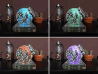
This is a project that i worked out together with my wife, who loves working with glass mosaic.
I love working with LED lighting projects, so i thought: let's combine the 2 hobbies and try to make a kind of art-project combining electronics and glass mosaic.
Combining RGB-LEDs with transparent glass mosaic gives very nice lighting effects.
Working with glass is a challenge, because it is not easy to make holes in glass. So i needed to find a way to power the electronics inside of the glass work without making a hole for a power supply connector or to feed through a power cable. Inside of the glass work is a microcontroller that is used to slowly change the colour using an RGB-LED. The colour changing is very slow, so you don't see it changing when only watching a few seconds. The microcontroller and LED don't need much power, so i didn't need a very powerful wireless power transmitter. Furthermore, the power did not have to be transferred over a great distance, but only over a few centimeters = thickness of the base cover + the thickness of the glass work.
Besides that, i didn't want to make a hole in the base for a power switch, to switch the wireless power transmitter on or off. So i decided to use a capacitive touch/proximity sensor for this purpose, because this type of sensor works through glass and when the capacitive sensor area is made big enough, it can work over distances of multiple centimeters. The sensor has to be temperature stable, very sensitive and using a small amount of power, since it is powered continuously.
The result is a nice looking colour changing lamp using wireless power transfer and that is be switched on/off using a capacitive proximity/touch-sensitive toggle switch.
System diagram of the project :
https://www.elektormagazine.nl/image/original/73136
Capacitive sensor including toggle switch (schematic1)
https://www.elektormagazine.nl/image/original/73137
The capacitive sensor circuit was published in Elektor Elektor Nr. 537/538 July/Aug. 2008.
It is a very stable and sensitive capacitive sensor, that can sense capacitance differences down to picofarads.
The circuit has virtually no problem with temperature changes, because the capacitance is measured using a differential approach, meaning that 2 signals are compared with each other. Both signals have the same temperature response, so this effect is cancelled out.
The relaxation oscillator build around U2B has a 50% duty cycle square wave output with a frequency of about 100 kHz. The output signal is fed to two RC networks, that both integrate the square wave signal. One RC network is fixed and formed by R2 and C1. The other RC network is formed by R4 and the capacitive sensor, that is made out of a copper clad PCB. The time constant of this last RC network will change with the capacitance between the copper clad PCB and earth.When capacitance is added, f.e. by moving your hand close to the copper clad PCB, the charge time of the RC network will increase, causing a delay, compared with charge time of the fixed RC network (R2/C1). The difference in charge times (thus delay) will be proportional to the extra amount of capacitance "felt" by the copper clad PCB. The compare operation, to measure this delay, can be done with an XOR. By feeding both signals to the 2 inputs of the XOR, the output of the XOR will show pulses with a width corresponding to the delay between the two RC networks. But the XOR will output pulses when the time constant of the capacitive sensor RC network is higher but also when it is lower than the time constant of the fixed RC network.
When we use a D-flipflop (U3A) to measure the delay, it will only output pulses when the clock input signal (CLK) is delayed, compared with the data input signal (D). When the D signal is delayed towards the CLK signal, the output will be 0.
R3 and C2 form an integrator with a very high time constant compared with the pulsewidth of the output pulses of U3A. So the voltage over C2 will be proportional with the pulse width of the output pulses. This means that the voltage will be proportional to the capacitance difference or in other words, the added capacitance.
U3B will toggle each time the voltage over C2 reaches the threshold voltage of the CLK input of U3B, which is about 1.5V. MOSFET Q1 is used as a switch that will toggle each time when the capacitive sensor sees enough extra capacitance. The MOSFET switches the +15V to the next stage, which is the buck converter for the wireless power transmitter.
R2 has to be adjusted so the U2A does not output pulses when the capacitive sensor does not "feel" any extra capacitance.
The capacitive sensor is very sensitive and will react to any change in capacitance. So when you connect the ground-clip of your scope-probe to the circuit, the total capacitance "felt" by the sensor is changed. The same thing when you connect the circuit to a lab power supply that is earthed. This will also change the total capacitance "felt" by the sensor.
So it is important to adjust R2 in the situation in which the capacitive sensor will be used without connection a scope. Best is to put a LED at the output of U3A, so you have a visible indication of the capacitance.
Once R2 is adjusted adjusted and you move the sensor over to another table made out of other material or that is higher, lower, thicker or closer to a wall, the capacitance will change and you have to re-adjust R2. Also when you re-route the power cable coming from the adapter to power the lamp, this might influence the capacitance, especially when routing it close to a wall or metallic objects.
Buck converter (schematic2)
https://www.elektormagazine.nl/image/original/73138
The buck converter is used to bring the power supply down to about 5V for the wireless power transmitter. With 5V, the transmitter delivered enough power for my purpose.
The microcontroller that controls the RGB-LED and the RGB-LED itself do not need a lot of power. Furthermore, the distance between transmitter and receiver is maximum a few centimeters, so i did not need to burn a lot of power just to overcome the distance. This also keeps the temperature of the transmitter components cool, because the whole thing is assembled in a completely closed enclosure without any air vents.
The buck converter is nothing special. See application note for the MC34063. I added an extra buffer (Q1, Q2) and switching MOSFET, because i noticed that the chip got pretty warm
when pulling 1A continuously. So i over-dimensioned the switching stage to keep the temperature of the chip down. Probably it was not a problem at all, but i prefer to keep things safe,
especially because the magic lamp is connected to the power supply day and night and sometimes one of our cats adds enough capacitance to switch on the magic lamp on.
Wireless power oscillator (schematic3)
https://www.elektormagazine.nl/image/original/73139
I used a Mazilli ZVS oscillator for a project involving wireless power transfer.
I used an adapter as a power supply to power the Mazilly oscillator, but i noticed that the oscillator didn't always start.
When the oscillator does not start, one of the FETs latches into conduction and remains conducting while the other FET stays open.
After a while the result is the distinctive smell that every electronics engineer immediately recognizes, knowing that something got hotter than planned.
I discovered that the problem was due to the slow and irregular startup of the power supply.
The power supply voltage did not rise fast enough and had some bumps down the road.
So the choice was either to find a power supply that had a faster startup time or to find a solution that would allow slow starting power supplies.
The last choice is of course the best one, but not the easiest.
I solved the issue using a time delay, that ensures that the 100E MOSFET gate resistors are connected
about 250ms later to the power supply than both the drains of the MOSFETs.
The time delay circuit is built using transistors. Q2 and Q3 form a differential amplifier. At power on, R1 will start charging C6. The voltage over C6 rises untill the threshold voltage, that is set by R3 and R7 is reached. At that moment, Q2 will start conducting and pulls the base of Q1 low. This means that Q1 will start conducting and thereby connecting the 100E MOSFET gate resistors to the power supply. Both MOSFETs will turn on, but only one MOSFET can win the race. The winner will start conducting and will block the other MOSFET via the schottky diode.
C1 and C3 are only assembled for tuning of the LC circuit. They can be assembled to make small adjustments when tuning of the resonance frequency is necessary.
The coil is made of 14 turns of 1mm diameter enamelled copper wire, with the windings wound on top of eachother. The height of the stacked windings is about 16mm.
The total inductance of the coil is about 16 uH.The diameter of the coil is about 57mm.
The coil is tapped right in the middle by removing the enamel and soldering a tap-wire. You can also wind two separate coils of 7 turns and join 1 side of both coils together,
but then pay attention that both coils have the same phase. When the coils are connected in opposite phase, the total power will be close to zero.
Together with C4 and C5, with a total capacitance of 200nF, the LC network results in a resonance frequency of about 81 KHz.
It does not matter if the resonance frequency is higher or lower when you build this circuit, as long as the transmitter and receiver use the same resonance frequency.
Wireless power receiver (Schematic4)
https://www.elektormagazine.nl/image/original/73140
C1 and C2 are only assembled when tuning of LC resonance frequency is necessary and small adjustments are needed.
The coil is made of 14 turns of 1mm diameter enamelled copper wire, with the windings wound on top of eachother. The height of the stacked windings is about 16mm.
The total inductance of the coil is about 16 uH.The diameter of the coil is about 57mm. This coil doesn't need a tap.
D1 is a schottky diode that is used as a half wave rectifier. You can also use a full wave rectifier, but this will eat away more voltage from the incoming signal because then you loose 2 diode-drops.
U1 is a 5V ultra low drop voltage regulator with a typical dropout voltage of 0.6V/1A, so it will work down to an input voltage of 5,6V at 1A.
RGB-LED controller with Microchip PIC12F683 (schematic5)
https://www.elektormagazine.nl/image/original/73141
The RGB-LED controller is build around a Microchip PIC12F683.
The PIC12F683 uses a semi-random generator to change the colour of the RGB-LED randomly and very slowly, so you don't really notice the change when you look for a few seconds.
The firmware uses a kind of gamma-correction to linearize the brightness of the LEDs so the colour change is very smooth and linear.
P.S.: The hex file for the PIC will be uploaded later in a project update, because it is an "old" project of mine and i have to dig out the source code and compiler to check if i can regenerate the hex file.
Power consumption
The total current consumption of the magic lamp is about 150 mA at 15V with the wireless power transmitter switched on and the RGB-LED lit up.
When removing the wireless power receiver, the current consumption is about 94 mA, so the receiver consumes about 60 mA at 5V for the RGB-LED and the PIC12F683.
When the transmitter is switched off, only the touch sensor is connected to the power supply and draws about 5 uA, so virtually nothing.
Power delivery of the wireless power system
I could draw a maximum of 250mA from the wireless receiver before the ultra low drop regulator dropped out, with the wireless receiver coil a few centimeters straight above the wireless transmitter coil. Maybe with precise tuning of the resonance frequencies of the transmitter and receiver LC networks, the power delivery can be optimized and increased. But for this project the power delivery is more than sufficient.
I got this magic lamp continuously plugged in for years now and it never let me down.
Enjoy !
Want to build a project?
Bring your design to life with the Elektor PCB Service, powered by Eurocircuits. Upload the project files and order professionally manufactured PCBs or assembled boards through a proven European production platform.
Supporting KiCad, Eagle, Gerber, and ODB++ formats, the service is suitable for everything from prototypes and validation builds to series production and volume manufacturing.
Made in Europe. Fast. Reliable. Professional.
Updates des Autors