
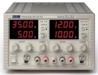
Lab Power Supply 0-40V / 0-2A [120437]
It should have display of voltage and current. It's often I would need PSU like this but I haven't found any chematics with voltage up to 40V. If it's possible to do with PIC microcontroller it would be nice.Next follows up on ‘Elektor lab design’ from 3 September 2012.
It should have display of voltage and current. It's often I would need PSU like this but I haven't found any chematics with voltage up to 40V. If it's possible to do with PIC microcontroller it would be nice.
Next follows up on ‘Elektor lab design’ from 3 September 2012.
We finished the main part of the power supply. A microcontroller for adjusting voltage and current and display the readings has not been chosen yet. The design still uses the LM5117, but instead of the analog filter stage to filter out the switching artifacts we chose a linear amplifier. The filter was not able to suppress all fluctuations from the SMPS, especially at low loads when pulse skipping occurs. Also the amplifier is better at suppressing voltage variations caused by large load variations (for instance high current low frequency pulses). To protect the amplifier it is has its own current limitation, which sets in at around 2.5 A. This is the reason we abandoned a first idea to see if we can increase the maximum current output at low output voltages. The maximum is now 2 A overall.
Before looking for components it has to be clear what kind of power supply it is going to be. Because of the wide output range from 0 to 40 V a standard linear concept is not very sensible. At maximum output current a linear design will dissipate 80 W, maybe even more. A large heat sink is required or a sufficient forced cooling to handle the maximum loss indefinite (having it shut down after a while is not practical). Or if the input voltage is changed at fixed levels (some power supplies do) the power loss can be halved or more. But the loss will still be high. So we went for a switched mode power supply. Big plus of a SMPS is its efficiency. But the output voltage always has a ripple and switching artifacts. So the first idea was to put a simple buffered filter at the output to suppress these to an acceptable level. This of course doesn’t change the design of the SMPS. Looking for Synchronous Buck Controllers the choice for ones that can handle 48 V or more are not that common. We finally came across the LM5117 simply by sifting through several manufactures product selectors and entering the necessary specs. By selecting Light Load Efficiency only the LM5117 was left… It looked simple enough for our needs. We’re not going to sum up all its features (please read the datasheet and Application Note 2103 LM5117 Evaluation Board at www.ti.com first) but we will explain the choice for the components in our design.
The values for resistor divider R1/R2 (under-voltage lock-out) are selected for 1 V hysteresis and 44 V as startup voltage. The calculated values are rounded to the nearest E96 values. The startup voltage is with present values about 43.7 V. The capacitor for decoupling (C1) is larger than recommended but we chose a better suppression of the switching noise.
We chose a lower switching frequency as the standard application, 100 kHz. It will generate less HF-noise, since our PCB design is only double sided. Also the switching losses will be less. But maybe more importantly at 100 kHz the maximum duty cycle is about 96 %. The SMPS is able to deliver a high enough voltage to the linear output amplifier from a standard 48 V power source. The calculated value for R4 (RT) is 51.052 kΩ. This is very close to 51 kΩ (E24) or 51.1 kΩ (E96), we chose the first.
A prolonged soft start is not needed so it is only 37.6 ms. The value of soft start capacitor C4 can be relatively low, 470 nF.
We recommend leaving the diode emulation pin open (jumper JP1, DEMB). This will give less power loss under light load conditions.
The parameters for the formula of the output inductor (L1) are all known, although we don’t have a variable input voltage. It's fixed at 48 V. We also chose a ripple current of 40 % of the maximum output current, so 0.8 A. The calculated inductor value is 83.33 µH. This is very close to an E12 value. The inductor we chose is from Würth Elektronik. It is slightly overrated for our purpose but it will therefore ensure a minimum power loss in the output inductor. It can handle more double the output current needed without a decrease of its inductance (saturation is specified at 8.5 A). In principle the SMPS part of the power supply is capable of delivering a lot more than needed. With a DC resistance of only 30.4 mΩ the power loss is minimal (not mentioning the core losses).
The maximum output current of the SMPS part of the design is intentionally a lot higher than the linear output part will ever be able to supply. This way the SMPS will have less influence on the regulation of the power supply as a whole, particularly when the power supply is in current control mode. We’ve chosen 12 A as a current limit. This may seem far too high but testing at lower limits gave a less stable performance. The inductance of the output inductor is at 12 A about17 µH, so not really a short circuit yet. In principle the condition where these current levels will take place is only possible if the linear output amplifier is damaged. The calculation of the peak inductor current doesn’t need to be that exact. The factor determined by the minimum ON time in the formula is in our case less than 0.3 A (taking the drop to 17 µH into account). In our case the resistor needed (R9) has a nice standard value of 0.01 Ω.
The datasheet mentions the current sense filter not really being necessary. We added it none the less (R7, R8 and C8) but kept the resistor values very low not to influence the current sense amplifier gain. With 1 nF for C8 it filters out only very high frequency artifacts.
For the ramp capacitor C7 we chose 1 nF (halve of the maximum value). A high value will be less receptive to external disturbances. The ramp resistor needed according to the formula would have to be 820 kΩ. During testing a resistor of 1.2 MΩ gave a more stable regulation at different output voltages.
For the decoupling capacitors C9 (for VCC) and C10 (HB) we kept the value from the datasheet. There’s no reason to change them. The diode used for the bootstrap (D1) has a very low voltage drop (at 1 A 0.57 V typ.).
The MOSFETs from NXP for the power switches (T1/T2) used in the design example in the datasheet are simply perfect. We think better ones will be hard to find. The gate resistors prevent parasitic oscillation but also influence dead time. Adding the resistor decreases dead time. But since the source current from both LO and HO outputs is less than the sink current T1 and T2 are turned off faster than they are turned on. With 2.7 Ω gate resistors the gate current is 2.8 A when sinking (at 7.6 V VCC, driver output resistance is not specified). The source current is only 2.2 A maximum.
The snubber network R13 and C12 has not been changed much. The resistor value remained the same, only the capacitor value is doubled to compensate for the increased inductor value en lower switching frequency. The signal between T1and T2 is free from ringing and spikes.
The output capacitor was selected to have a low ESR, high ripple current (2.77 A at 100 kHz) and longevity (3000 h at 105 °C). The high ripple current is also needed to withstand high pulse loads. Theoretically the ripple voltage across C13 would be in the order of 1 mV if only the capacitance is considered and its ESR 0 Ω. But measurement at maximum load and 20 V out shows a ripple voltage of 40 mV or so. The impedance of the capacitor rated 36.5 mΩ. Even with the parallel circuiting of C14…C16 the ripple voltage is a lot higher than we would like it to be, just the reason to have a linear output stage.
To decouple the source power supply the capacitors in the input must have a very low ESR and withstand high peak currents. C2 and C26 have an ESR of 27 mΩ and can handle almost 2 A at 100 kHz. Additionally are SMDs in parallel for the higher frequency range. This will ensure a very low ripple voltage at the input. To make sure virtually no ripple gets thru an extra inductor of 10 µH is added (L2). With an oscilloscope it’s hard to make out any ripple. This way there no high frequency loading of the capacitor of the source power supply. Usually high frequency pulse loading is not specified. To keep the extra power loss in the inductor to a minimum a type with a DC resistance of only 14.1 mΩ is selected.
The internal voltage regulator (7.6 V typically) is not supplied by the main input voltage but by the separate power supply for the control circuit. This is a much lower voltage. So the power loss in IC1 is much lower. The filter (R12/C11) to avoid high frequency switching noise injection also works the other way around. Noise from IC1 to the control circuit power supply is suppressed.
The LM5117 has three different reset modes: hiccup, latch-off and cycle-by-cycle. While testing and experimenting with a proof of concept we think hiccup is the best choice although latch-off is safer. In latter case you have to press the reset button (S1) or turn the power supply off and on again. C3 controls the time a soft-start takes after the exceeding of a current limit. For those who like to experiment or simply have a different opinion JP2 sets the three different reset modes. The modes are clearly indicated on the PCB. In case you’re not sure, no jumper selects hiccup.
The CM output of the LM5117 provides average output current information but is only valid in continuous conduction operation. It is made available on K6 for testing purposes. R39 and C21 attenuate the sampling noise.
The one thing we really differ from the standard application and made the design ‘difficult’ is the feedback from the output. In the first design stages a buffered filter was used at the output, see schematic_1. +Vout was fed back to IC2A (through divider R22/R23). So the output of the SMPS had to go down to almost 0 V (the drop across the output filter had to do the rest). Without special measures the output of the LM5117 SMPS can only go as low as the internal reference, which is 0.8 V. Not really low enough at that time. To make the output voltage controllable we added opamp IC2A in the feedback. R27 and P2 compensate the 0.8 V reference voltage. Compensating the 0.8 V reference voltage has to be done with a certain precision and so a negative reference voltage was added (IC4). The – 5 V from a 7905 is not stable enough. P2 was the original offset correction but can now be used to shift the SMPS voltage a little (if needed). Schottky diode D3 prevents the output of IC2A ever becoming too negative. The LM5117 doesn’t react well when this happens. In schematic_2 is shown a simplified schematic of the correcting amplifier (IC2A) and the internal gain from the LM5117. The gain from IC1 is set by R4 and R5. By changing the ratio of R4 and R5 it easy to calculate the influence the gain of the LM5117 has on the value for R6 (R22 in the main schematic). This is the resistor we need to determine. The gain is has to be 10 times (Uout/U1). The value for R2 is easy to calculate. If U1 is 0 V than the output of IC2A should be the same as the internal reference of the LM5117. So R2 = 2.5/(0.8/R3) where 2.5 is the reference voltage of IC4.
Some equations (the offset of 0.8 V at the output of IC2A is ignored):
U1 = Uout/10
U2 = R7/(R6+R7)*Uout
U3 = R4/R5*Uout
Rx = the parallel value of R1 and R2
U3 = -(R3/R1)*U1 + (1+R3/Rx)*(R7/(R6+R7))*Uout
After substitution we can calculate R6:
R6 = (R7*(1+R3/Rx))/((R3*U1)/(R1*Uout) + (R4/R5)) – R7
If we presume the gain of IC1 to be 1000 then R6 is 43.94 kΩ. If the gain of IC1 is 10000 then R6 is 44.35 kΩ. We chose an E96 value of 44.2 kΩ. If the DC gain of IC 1 is a lot higher, let’s say infinite, than the total gain will be lower than 10 times. 9.9569 to be precise. A control voltage of 4 V will result in an output voltage (Vsmps) of 39.83V. The output amplier has a voltage across large enough not be influenced by this lower gain.
Because of the altered feedback configuration the formulas for the loop compensation components are no longer applicable. We tested different component values and eventually found the present values to be the best compromise. We still have the impression at both ends of the output voltage range the values should be a little bit different. Maybe that’s the reason only applications with a fixed output are presented.
Setting the output voltage and maximum current limit is done by onboard potentiometers (multiturn) or a microcontroller. With jumpers JP4 and JP5 a selection can be made for each separately. The selection made by JP4 for the voltage setting is buffered by IC2B. A resistor (R24) is placed in series with its output to enable current limiting. A transistor (T3) pulls the signal to ground if the set current limit is exceeded. If jumper JP3 is removed the current limit will have to rely on the microcontroller only. Opamp IC2D compares the level present at JP5 with the measured current in the output. To make the current control stable gain and bandwidth are limited (R33, R34 and C22). Schottky diode limits the output of IC2D if the limit is not reached. Reaction time is reduced when the current control reacts. The output doesn’t have to rise from -5 V but from 0.14 V (a value from our prototype) below the measurement value of the output current (1 V/A). At 1.86 V transistor T3 will become slightly conducting. Voltage divider R35/R36 reduces the voltage on the base of T3 to 0.43 V. The value of 470 Ω for R38 puts 2.5 V on P4 so the current level can be set higher (2.5 A) than the design is meant for. At a setting higher than 2 A T3 will start reducing the output voltage and the relation between the voltage setting (P3 or microcontroller) and output voltage will not be linear. Of course software could compensate for this…
As we told at the beginning of this document the linear amplifier attenuates the ripple from the SMPS. To save power we want the drop across the output transistor of the linear amplifier to be low at all voltage settings. This means the SMPS always has to have a slightly higher voltage than the linear amplifier output. We decided to make the drop across the output transistor 2.5 V. This is achieved by IC2C and D4. The voltage to the amplifier (R44) is the same as the voltage derived from JP4. The voltage to the SMPS (R25) is the voltage drop across D4 higher. R43 sets the current through D4 and thus the level of the voltage across D4. At 0 V (5 V across R43) the drop in our prototype was 0.252 V and at 40 V out (9 V across R43) the drop is 0.268 V. That’s constant enough for our purpose. Since the SMPS and the amplifier both have a gain of 10 this differential is amplified 10 times and the voltage across T4 will more or less vary from 2.52 to 2.68 V. The power loss in T4 will be 0.32 W higher and the temperature of the heat sink 2 °C higher at maximum voltage and current output.
The linear output amplifier is basically an opamp (IC7) with a power MOSFET (T4) as a buffer at the output. With a MOSFET at the output current can also flow in reverse direction without harming the transistor, provided the current isn’t too high. In case of a source follower design (N-channel MOSFET) a current dependent voltage drop across T4 would occur and furthermore the voltage swing from IC7 would increase this voltage drop even more. So a common-source circuit with a P-channel MOSFET is the only alternative. In theory the gate turn off voltage of the MOSFET (-2 V minimal) can be less than the voltage swing of the opamp towards the positive supply rail. A voltage divider (R51/R52) is used to control the gate voltage. But the divisor is minimal. Should for one reason or another IC7 be absent, R52 will make sure the MOSFET is turned off. Since the DC loading of the opamp is minimal the voltage swing of the opamp is about 1.5 V below its positive supply rail. According to the datasheet this is 2.7 V worst case, but this means in practice it will still be low enough for the MOSFET to be fully turned off by IC7. To speed up the control loop a RC network is placed in parallel with R51 (R50 and C47). C47 is several time the input capacitance of the used MOSFET (AUIRF9540N). This input capacitance is 1300 pF. The opamp (OPA552) is no ordinary one. It can handle supply voltages from +/- 4 V up to +/- 30 V with very high output current capability (200 mA). There is another version that’s unity gain stable (OPA551), but since gain of the amplifier has to be 10 times we selected the faster one. At 0 V output the gate voltage has to be lower than ground level. That’s why the opamps negative supply rail is connected to the -5V. At a swing of 1.5 V from the -5 V supply the output voltage of IC7 can be -3.5 V. The voltage drop of T4 (2.6 V) plus the minimum output voltage of IC7 (-3.5 V) makes a total of -6.1V. That makes the gate voltage of T4 maximal 5 V. This is enough for all practical purposes but not very realistic. What is the minimum voltage at which we need 2A? We think 1V or so. Below this voltage the maximum current is not guaranteed. At 2 A there is an extra voltage drop across R57! R45, R46 and C46 make the control stable, this is also important when the power supply is in current control mode. The control loop is more complex then. R49 and C48 also stabilize the output, especially transient from pulse loads. C45 filters the input of the amplifier but also is part of the components that stabilize the control loop in current control mode. C51 suppresses high frequency noise. A shunt (R17) is placed in series with the outputs positive power supply rail to measure the output current. This way all ground levels are directly connected. C18 and C17 filter the output. To compensate the increase in output impedance (the addition of R17) the feedback from the amplifier (R47, R48 and P1) is taken directly from the output connecter K2. This way all resistance in the output up to the solder joint of the screw terminal K2 is compensated. P1 is added to exactly trim the output to the set output voltage. With a microcontroller this could also be done by software. Feedback ground is taken from a star point at the heat sink. From here a large copper plane ensures virtually no voltage drop. To really protect the output transistor from a short circuit it has to have its own current protection. This is done the old fashioned way but still the best way (and it takes only a few components). A resistor (R57) in the source is connected to the base and emitter of a PNP-transistor (T5). When the voltage across R57 gets to 0.6 V the transistor will start to limit the gate source voltage. With a value of 0.22 V this will happen at about 2.7 A, but probably a little earlier. This is a very fast way of current limiting and the microcontroller should be able to reduce the voltage fast enough to prevent the heat sink from heating up to high. The voltage across T4 will become larger than 2.6 V if no correction by the microcontroller follows. A similar story goes for the voltage across T4. Should it ever get to large D9 will enable T6 and the gate source voltage will be reduced also. A possibility could be when the SMPS voltage is too high, but the microcontroller should correct or report this. In stand-alone (without the microcontroller board), this is more conceivable. JP6 enables this extra protection.
A little story about C17. Originally it was used in the output filter concept that was rejected (schematic_1). For this purpose the capacitor has to have a very low series resistance. Ordinary electrolytic capacitors are unsuitable. They often have series resistances in the order of 1 Ω or worse. Also the ripple current is usually in the order of mA. So we had to look for one with a series resistance in the order of mΩ and higher ripple current specification. From past experience we know that Nichicon is a manufacturer that makes excellent electrolytic capacitors. We chose one from their LX series. The 50 V/47 µF version has an ESR of 29 mΩ and a rated ripple current of 2.6 A (below 105 °C), both at 100 kHz. With these specifications it is also an excellent output capacitor. Only downside of the capacitor is its rated leakage current, almost 0.5 mA. But if we understand the datasheet correctly this is at maximum rated voltage and 105 °C.
The output current is measured across R17 by IC3, a current sense amplifier from Linear Technology with extended input range. Absolute input range is 44 V while the IC itself can be powered from 5 V only. For a detailed description we refer to the datasheet. The gain is set by the ratio of R20 and the value of R18 (R19). We chose a gain of 20. This way using a current sense resistor of 0.05 Ω the output voltage across R20 is 1 V/A. Since our maximum output current is 2 A, a 1 W version for R17 can withstand more than twice the maximum current continuously. So it won’t burn out that easily in case anything’s wrong. The input power supply can deliver 3.2 A, but at a lower voltage setting the SMPS can deliver more. We plan a 3 digit display reading for both voltage and current. A reason for this of course is the accuracy of the current measurement with IC1 and the voltage divider for the measurement of the output voltage consists of 1 % resistors. Also the current through the feedback is not negligible. With no load we measured the voltage across R20 at increasing output voltages and calculated the error of the sense amplifier:
Uout UR20 IR47 IR30 Error
5 V 4.42 mV 0.25 mA 0.25 mA 3.92 mA
10 V 4.78 mV 0.5 mA 0.5 mA 3.78 mA
20 V 5.94 mV 1 mA 1 mA 3.94 mA
30 V 7.26 mV 1.5 mA 1.5 mA 4.26 mA
40 V 8.61 mV 2 mA 2 mA 4.61 mA
From the table it’s clear that from 20 V or so the error is not constant (unknown is the influence of the leakage current of C17). Theoretically it can be measured and by interpolation subtracted from the reading by the processor. These errors won’t be the same for other power supplies though. A calibration procedure could be an option. A simpler way is ignoring it by using a 3 digit reading.
To avoid any additional disturbances, noise generators and switching artifacts we used a small old fashioned linear power supply design to power IC1, IC2 and IC3 and other parts of the circuit. Standard regulators 7805 and 7905 are used. To protect the output of the negative regulator from being pulled to the positive supply a schottky diode is placed at its output. If the input voltage of a 7905 regulator drops below its output voltage (in absolute sense) the output gets into a high impedance state. When the power supply is switch off the output of the 7905 will be clamped to about +0.2 V. The +5V and -5V are available for the processor also (K3). Leds D5 and D6 show if these supply voltages are present, but also if the mains voltage is connected to K4. K5 makes it easy to connect the external power supply, simplifies the wiring of the mains voltage. The transformer has two primary windings, so it is suitable for 115 V and 230 V mains voltages. On the PCB one wire bridge (JP7) has to be placed to configure it for 230 V (JP8 and JP9 must be left open!). The two other wire bridges (JP8, JP9) need to be placed to configure it for 115 V (in this case JP7 must be left open!). Fuse F1 is an extra safety measure; you never know what might happen with the external power supply.
If the mains voltage is disconnected and the +5 V and -5 V are too low IC2 will no longer function properly. If not prevented the control voltage will go higher at low voltage settings (below 3 V). To prevent the output voltage from rising above the set value the input of IC7 is shorted to ground by a junction fet (T7). T7 is a PMBFJ110 from NXP and has a gate-source cut-off voltage somewhere between -4 V and -0.5 V (VGSoff). The gate is directly connected to the – 5 V. As soon as the – 5 V decreases and becomes equal to VGSoff T7 will start to limit the control voltage of the output amplifier and the output voltage will drop. At 0 V gate-source voltage the drain-source on-state resistance is maximal 18 Ω. The control voltage will be attenuated at least a hundred times. Any output voltage will be reduced to a save level no matter what the output level before switching off the power supply was.
As mentioned earlier the power supply for IC1 (VIN, pin20) is taken from the linear power supply to reduce unnecessary power loss in the linear regulator in IC1. To keep the voltage across C44 as high as possible and the ripple minimal the capacitor value is much higher than it usually would be chosen. Also the rectifiers are schottky diodes with very low voltage drop (at 100 mA less than 0.3 V). The ripple across C44 in our prototype is about 100 mVpp (100 Hz) at 17 VDC (depends on the exact mains voltage). Also this DC voltage will be lower once the microcontroller board is connected. In our prototype the current drawn by VIN was about 13.9 mA.
An important aspect of the output amplifier is the power supply of IC7. The positive power supply of IC7 has to be the same as the output amplifiers. But the minimum operating power supply of the OPA551 is +/-4 V. So if the output is 0 V and the positive power supply of IC is directly connected to Vsmps’ this would result in a total of 7.6 V across IC7. Well maybe in practice this can be enough but we didn’t take the chance. So below an output voltage of about 2.4 V the positive power supply of IC7 is taken over by the +5 V power supply. D11 and D12 make sure no current can flow between the +5 V power supply and Vsmps’. L3 suppresses possible switching artifacts present in the Vsmps’ power supply. In our prototype the voltage drop across D11 and D12 is just below 0.2 V.
All relevant signals to the microcontroller board including power supplies are connected to header K3. Pin1 is the output of the current sense amplifier. Any extra parallel resistance on the microcontroller board will influence the accuracy of the current measurement. Best is to place a buffer with a high impedance buffer on the microcontroller board. Same is true for measurement of the output voltage (pin 3, R30 and R31), the voltage of the SMPS (pin11, R58 and R59) and the external power supply voltage (pin 13, R14 and R15). Resistors R30 and R31 divide the output voltage exactly by 10. So the maximum voltage here is 4 V, only question now is if this is not too high for the microcontroller. Placing 1.8 kΩ parallel to R31 on the microcontroller board would halve this voltage. The same is true for divider R58/R59. The voltage on pin3 would then be 0.05 V/V. Since the external power supply is a constant 48 V resistors R14 and R15 divide this voltage to exactly 1 V. Since an exact measurement is not really needed the detection of a deviation is enough. Choosing a random division is of course easy to correct if a 10 or 12 bit A/D converters are used. Originally divider R30/R31 was buffered by IC2 but an extra opamp was needed to implement the voltage drop across T4. We kept the extra resistor (R32) at the output and extra decoupling with C20, because this measurement should be accurate. An extra capacitor on the microcontroller board can give an extra decoupling of HF noise. Small fluctuations in the measurements of the external power supply and the SMPS voltage are not to be considered errors. If necessary in software any disturbance can be filtered out. Speed is not an issue here.
What should the microcontroller board have?
To measure the four readings (Vout, Iout, Vsmps’, Vin) from K3: 4 x A/D 12 bit (0 to +5 V range)
2 x 16 or 4 x16 LCD
Supply 2 control voltages for Vout and Iout to K3: 2 x D/A 12 bit (Vout 0…4 V, Iout 0…2 V)
Two rotary encoders with pushbuttons to set Vout and Iout limit and change menu settings
Pushbutton to immediately set the output to 0 V
Led to indicate current control mode is active (or flashing backlight?)
Buffers to and from K3 to protect the processor and maintain accuracy (low offset, MOSFET, R/R-I/O)
Buzzer for warnings and power supply ready
Temperature sensor
Switch output for fan or other application (relay or opto coupler?)
Serial USB connector (our BOB?, where do we place it?)
ISP connector
What should the software do?
Display readings of Vout and Iout in 3 digits each (with calibration maybe 4 digits possible?)
Set Vout and Iout limit (by pressing the appropriate rotary encoder, back to displaying reading after 2 or 3 seconds)
Give choice between hardware current control only and software only (or both?)
Monitor Vin and Vsmsp. If readings are outside specified tolerance adjust output to 0 V and give warning (choices in menu to reactivate output: stay reset, press one of the rotary encoders or automatically after 5 seconds or so)
Monitor temperature (if possible close to heat sink (if > 35 °C activate fan or buzzer, selection by menu)
What we also would like:
Sub menu for current control by software only (peak, average or crest factor in percent)
Add-on?
A little PCB with a simple buck converter for fan (48 V to 5 V converter) and an extra space for the BOB and an USB socket for 5 V supply)
Update July 17, 2014
OK, this project is not one of our fastest advancing projects, but it is now more or less ready, because we finally finished the software. When you judge the software by what it shows on the display, you may be surprised by the time we took to write it, but there is more going on internally (and it was a low-priority job).
After powering on a splash window is displayed with the firmware version. Then the PSU enters Normal Mode in which it shows the voltage and current limit set by the user, the voltage and current measured on its outputs, the power delivered, a current crest factor and the temperature.
The output voltage and maximum current can be set with the rotary encoders. They have a sort of acceleration detection in the software, so that when you turn them fast, the controlled value changes quickly. When you spin slowly, you can control step by step. This allows you to go to 40V in a quick swing instead of turning the knob for hours.
The pushbutton will activate or deactivate the output. The LED is lighted when the output is active.
Pressing both rotary encoders will enter Setup Mode. Here you can change the LCD backlight timeout (the backlight is a bit heavy on the 5V power supply), (de)activate the buzzer, (de)activate the serial over USB port and the unit for the temperature display (C or F).
Now things become slightly more complicated. If you press the max current rotary encoder (right) you will enter Status Mode where you can check some internal parameters. If, on he other hand, you press the voltage encoder (left), you will enter Calibration Mode. This mode is needed to calibrate the ADC and DAC of the MCU. Without calibration the PSU is OK, but with calibration things get better.
All settings are stored in EEPROM. User settings are stored only when they have become stable for at least 10 seconds. This is to save EEPROM write cycles.
The USB port allows you to capture data from the PSU and to control its parameters from a terminal. You can use this to automate things if you like.
Internally the software samples the output voltage and current at 10 kHz and makes the measured values available after some filtering. For the current the RMS value is also calculated, which is needed to calculate the crest factor.
Current limiting is also done at this rate. If you prefer you can bypass this with a jumper and do current limiting in hardware. When the current limiting kicks in the buzzer starts beeping. Three short beeps at 1 Hz.
The rotary encoders are ticked on 100 Hz, the LCD is updated at 20 Hz.
That's all that I am going to write now.
Buy the PCBs in the Elektor shop:
Diskussion (8 Kommentare)