
High Speed USB 2.0 isolator
This is a concept for a high speed 480Mbps usb isolator.Why?Just try and find a high speed (480Mbps) usb 2.0 isolator anywhere.
This is a concept for a high speed 480Mbps usb isolator.
Why?
Just try and find a high speed (480Mbps) usb 2.0 isolator anywhere. Save from some fiberoptic medical systems, there are none.
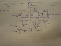
The reason for using the UTMI bus is because 480MHz digital isolators are not availible.
The UTMI bus parallises the usb bus resulting in a clock speed of 60MHz, which is manageble with todays digital isolator technology.
The FPGA has to manage the power output on the device side. And it acts as a buffer for both transmitters.
This is a challenge because both transmitters have their own clocks and are both the master on the bus.
So the buffer design will be tricky. Also because USB preforms bitstuffing there is no predictable datarate, some incomming bytes on the UTMI bus will be flagged as invalid.
How deep should the buffer be? The maximum inter packet delay is 736 bit times. In normal operation the transciever automatically preforms bit stuffing and NRTZ(non return to zero) encoding.
It is possible to switch that off when acting as a transmitter, but the FPGA would have to take on that task.
Synchronisation could become easier if the FPGA supplies a clock to the trancievers.
30 lines have to be isolated, because the digital isolators can't work bidirectionally.
80mA @ 3,3V each side. the USB transmitters 130mW @ 3,3V and 55mW @ 1,8V.
The USB trancievers are of the USB3250 type by SMCS
The FPGA is a 144-tqfp spartan 6 by Xilinx.
The digital isolators are of the SI8440BB-D-IS type, or similar.
Powersupply isolation could be done with an ADuM3070, MAX256, two SN6501's or something similar as a controller in combination with a compatible transformer.
USB tranciever datasheet: http://www.terraelectronica.ru/pdf/SMSC/USB3250.pdf
Update 07-01-2013:
I made a design for a test PCB to see how the three power isolators preform. See attached schematic and PDFs
Build This Project
Bring this design to life with the Elektor PCB Service, powered by Eurocircuits. Upload the project files and order professionally manufactured PCBs or assembled boards through a proven European production platform.
Supporting KiCad, Eagle, Gerber, and ODB++ formats, the service is suitable for everything from prototypes and validation builds to series production and volume manufacturing.
Made in Europe. Fast. Reliable. Professional.
Diskussion (1 Kommentar)