The analog input of an Espressif ESP32 doesn't seem very reactive in the very first part of its allowed range, with a lack of response, and a non-linearity in the whole range, consequently. The aim of this project is designing a specific analog interface to linearize the analog inputs of the ESP32 even for those low values, getting the most out of the ADC and with a remarkable linearity. With this project, you will also learn how to use the powerful MicroPython language to build a data acquisition and proce
In its original release, the Espressif ESP32 has two 12-bit Successive Approximation Register (SAR) ADCs which can convert up to 18 analog inputs (the ESP32-Cx and -Sx versions have ADCs with other specs). The maximum value to convert is equal to the internal reference value Vref. For the ESP32, it is about 1 V, but it can vary between 950 and 1100 mV. It is also possible to use voltages higher than Vref by attenuating the input. The ESP32 has four possible attenuation options [1], as shown in Table 1.
In my case, the default attenuation is 0 dB, with an input range of about 68 to 995 mV. For a better accuracy, it is recommended not to use attenuation (i.e., 0 dB) and to utilize the pins related to ADC1. I’ve used GPIO34.
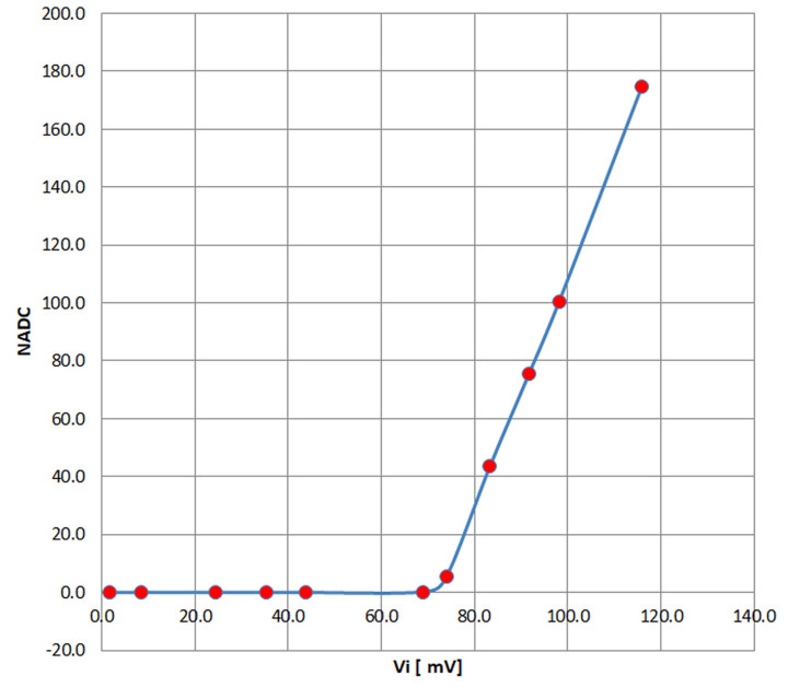
Figure 1 shows a fairly serious problem at low input levels: below 68 mV (in my case) the converter output returns zero, creating a dead-zone and strong non-linearity on the whole range.
Figure 1: This curve clearly shows the no-response zone between 0 mV and 68 mV, followed by a sharp ”knee”, impairing the overall linearity.
The Aim of the Project
The goal of this design is to achieve an extended input range from 0 V up to a maximum of 3 V or even more, whilst maintaining a perfect linearity. A summing amplifier circuit can meet this objective: for a zero input, it sums a voltage corresponding to the minimum value detected by the ESP32 so that its output might go to zero when the input of the circuit is effectively zero. The proposed circuit also extends the range to a maximum value of about three volts, easily increased by using a single resistor in series.
The Summing Amplifier
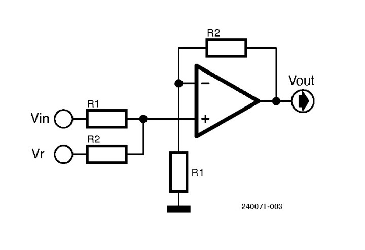
In Figure 2, we can see the single-supply, non-inverting summing amplifier, whose transfer function is as follows:
Vout =Vin ·R2 /R1 +VR ·R2 /R2
Figure 2: Single-supply summing amplifier.
Input Vin is the main input and must be reduced with a gain of less than one, so it must be R1 > R2 with a gain of about 1/3. We also want the reference input VR, which will be summed with the attenuated input signal, not to be amplified.
Setting R1 = 330 kΩ and R2 = 100 kΩ in the previous equation, we obtain:
Vout =Vin ·R2 /R1 +VR =0.303·Vin +VR
If 68 mV is the value that brings the output to digital zero (other ESP32 may have slightly other values), we can choose VR = 68 mV. Then we have the following conditions:
ForVin =0mVVout =68mV and the ADC output is zero
ForVin =3000mVVout =977.1mV and the ADC output is near the max value
These conditions fully meet our prerequisites (i.e., having a good response and linearity from the ESP32’s internal ADC — even at input voltages ranging between 0 mV to 3000 mV).
The Circuit
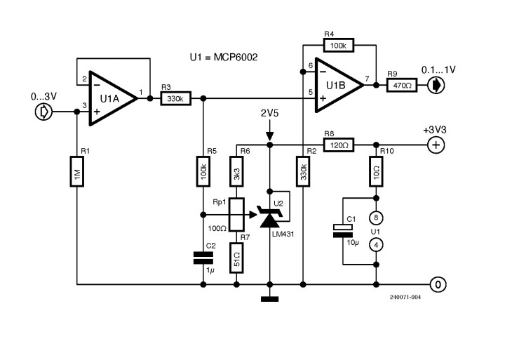
The complete interface circuit is shown in Figure 3.
Figure 3: The input interface circuit.
The operational amplifier U1A serves as a voltage follower, with very high input impedance and very low output impedance. The 1 MΩ resistor R1 avoids a floating input, and it is also very useful if we want to increase the input range. For example, putting a 10 MΩ resistor in series realizes a voltage divider of 1/11, extending the input range to 33 V.
The op-amp U1B is a summing amplifier (for more insights you might take a look at [2], page 4), and U2 provides a stable reference voltage. The VR voltage, present at the hot side of C2, is realized through a voltage divider and a trimmer, preferably a multi-turn type. This allows zero to be made at the output of the ADC. With the given values of voltage divider of the reference source U2, the VR voltage is configurable from about 37 mV to 116 mV. The capacitor C2 is recommended by the manufacturer of the 2.5 V voltage reference LM431, for a better suppression of the internally generated noise.
Rail-to-rail operational amplifiers, such as the one indicated, are particularly suitable for this application. I don’t recommend using operational amplifiers such as LM358; these, although indicated as suitable for single supply operation, do not work with input voltages below a few tens of millivolt.
Calibration
Now we need to perform a calibration. First we’ve to write a program that reads the values of an analog pin, in my case IO34, and prints them. We may use the Arduino IDE, the simplest choice, or MicroPython.
I used MicroPython because on my ESP32 development board I already had it loaded; if you want to choose this solution and learn this powerful language, you have to load it on ESP32 by following the instructions made available on various websites.
Then we place a jumper between the input and ground for Vin = 0, and start turning slowly Rp1 trimmer until we begin to see numbers other than zero.
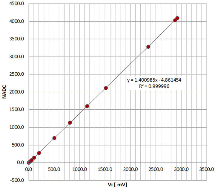
Connect the Vin input to a low-noise, stable voltage generator, checking the voltage with an accurate digital voltmeter, and take the various measurements and put them on an Excel-like spreadsheet to do a linear regression like the one shown in Figure 4.
Figure 4: The perfectly linear response of the ADC, after having implemented this interface at the analog input of the ESP32.
Seven to 10 measurements taken with a precision voltmeter are enough to obtain the coefficients with a linear regression, done with Excel or other programs. As can be seen, the results were excellent, with an R2 very close to one, in my case (R2 = R3 = 300 kΩ). The maximum input value that brought the output of the ADC to 4095 was 2923 mV.
To get the voltage in millivolts in our software, we need to invert the axes of the regression and insert the following expression in the code:
mV = NADC * 0.713780799 + 3.473077
Obviously, these values were applicable in my case, but might vary according to the components’ tolerances in your designs.
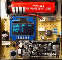
The Prototype
Figure 5 shows the circuit included in my development system that also has an OLED display and an IR receiver to decode TV remote controls. Only the input linearizer circuit, visible on the right of the photo, is described in this article, and the printout of the program listed are made using the USB serial instead of the OLED display, as pictured.
Figure 5: The finished prototype at work. The display on the left is not making part of this project.
Program
The program below, written in MicroPython, acquires 100 samples of channel GPIO34 at a sampling rate of 500 Hz (period = 2 ms) and then prints the sampling statistics. I took the average value while also observing the standard deviation of the measurements, which must be minimal.
# Program TestADSer.py to test display and ADC
# Giovanni Carrera, 03/03/2022
from machine import Pin,ADC
from time import sleep,sleep_ms
import math
ch1 = ADC(Pin(34)) # initializes the analog input
ndata = 100
arr = [0 for i in range(ndata)]
while True:
vmean = 0
vqmean = 0
ch1 = 0
vmin = 5000
for x in range(0,ndata):
arr[x] = int(ch1.read())
if arr[x] > vmax :
vmax = arr[x]
if arr[x] < vmin :
vmin = arr[x]
vmean += arr[x]
vqmean += arr[x]**2
sleep_ms(2)
vmean /= ndata # mean value
vqmean /= ndata # mean of quadratic values
k = vqmean - vmean**2
if k >= 0 :
StDev = math.sqrt(k)
else :
StDev = 0
print('Analog ch = IO34')
print('Max =' + str(vmax))
print('Min=' + str(vmin))
print('Mean=' + str('%.1f' %vmean))
print('Sdev=' + str('%.1f' %StDev))
print()
sleep(1)
The following instruction:
arr = [0 for i in range(ndata)]
is used to create the data buffer arr with size ndata.
In the acquisition loop, the sum vmean, the maximum vmax and the minimum vmin and also the sum of squares vqmean of the measurements are calculated. Next, the mean and standard deviation are calculated, which is equal to the square root of the mean of the squares minus the square of the mean. A check is also made on the sign of the radical k, which must be positive.
The sampling period, in milliseconds, is set by the following instruction:
sleep_ms(2)
Arduino Sketch
Those who wish to use the Arduino IDE can load into the ESP32 the sketch visible just below. To have the output precisely showing the voltage in millivolts, you must first do a calibration and adapt the values in your code (as described above for the Micropython software). The SW package for this design is available for download in the attachments section for this article.
/***************************************************************
program ESP32acq.ino
acquires ndata samples of analog channel pin 34
and calculates the maximum, minimum, mean and standard deviation
Giovanni Carrera, rev 04/12/2023
*****************************************************************/
uint32_t timep;
uint32_t deltat = 2;// period in ms
uint16_t value,NSamples;
uint16_t count= 0; // sample counter
#define ndata 100 // number of samples
#define ch1 34 // ESP32 GPIO34, ADC1_CH6
int16_t arr [ndata];// data buffer
[2] B. Baker, ”AN682 Using Single Supply Operational Amplifiers in Embedded Systems,” Microchip Technology Inc. , 2000: https://tinyurl.com/mr2nz8pu
Component List
Resistors
R1 = 1 M, 1%, metal film
R2, R3 = 330 k, 1%, metal film
R4, R5 = 100 k, 1%, metal film
R6 = 3.3 k, 1%, metal film
R7 = 51 Ω, 1%, metal film
R8 = 120 Ω, 5%
R9 = 470 Ω, 5%
R10 = 10 Ω, 5%
Rp1 = 100 Ω, multi-turn trimmer
Capacitors
C1 = 10 µF, 35 V, Aluminum electrolytic
C2 = 1 µF, 25 V, ceramic AVX
Semiconductors
U1 = MCP6002, dual rail-to-rail op amp
U2 = TL431, shunt voltage reference
Build This Project
Bring this design to life with the Elektor PCB Service, powered by Eurocircuits. Upload the project files and order professionally manufactured PCBs or assembled boards through a proven European production platform.
Supporting KiCad, Eagle, Gerber, and ODB++ formats, the service is suitable for everything from prototypes and validation builds to series production and volume manufacturing.
Das Elektor Magazine gehört seit 65 Jahren zu den führenden Informationsquellen für Elektronikingenieure, Entwickler, Start-ups und Unternehmen. Unser Magazin wird von einer aktiven Community aus Elektronikingenieuren – von Studenten bis zu Profis – getragen, die mit Leidenschaft innovative Ideen entwickeln und teilen.
Für diese veröffentlichen wir jedes Jahr Hunderte von Beiträgen in Formaten wie Artikeln, Videos, Webinaren und weiteren Lernformaten. Unsere Mission ist es, Wissen auf jede mögliche Weise zu teilen und die Leser mit den neuesten Entwicklungen im Bereich der Elektrotechnik zu inspirieren.
Vielen Dank für Ihre Bewertung!
Kommentar hinzufügen
Vielen Dank für Ihre Bewertung!
Möchten Sie einen Kommentar mit Ihrer Bewertung hinterlassen? Bitte melden Sie sich unten an. Nicht gewünscht? Dann schließen Sie einfach dieses Fenster.


Diskussion (0 Kommentare)