
FT311D Break-out Board [130516]
Based on a publication in Circuit Cellar (Unleash Your Android Device’s Potential, Issue #281, December 2013) we designed a little PCB to connect your phone or tablet to a breadboard or as part of a bigger PCB or project. The center of the circuit is the FT311D from FTDI, described as a USB Android Host IC.
Based on a publication in Circuit Cellar (Unleash Your Android Device’s Potential, Issue #281, December 2013) we designed a little PCB to connect your phone or tablet to a breadboard or as part of a bigger PCB or project. The center of the circuit is the FT311D from FTDI, described as a USB Android Host IC. There are some minor changes but the schematic is more or less the same. As a power supply connector we use a micro-USB connector, since the charger for your Android phone will have this type of connection for charging and applications. The FT311D is based on the philosophy not to draw any power from the Android device to spare the battery, hence the need for an external power supply. We called the function of LED1 “USB” instead of error, since a continuous illumination of the LED1 indication a good USB connection. Blinking means something’s wrong and if there’s no USB connection the LED is permanently off.
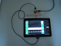
The PCB is relatively small; only 35.6 x 36.8 mm. Connection to an android device is by way off the old USB type A receptacle (K1). The phone or tablet will most likely have a cable supplied with it that can connect it to a USB type A receptacle. The interface of the FT311D is connected to a standard 2.54 mm spaced pin header (K2) on the opposite side of the PCB as where the USB type A receptacle is located. Using a special pin header with rounded pins and soldered to the bottom side of the PCB, it can be placed easily on a bread board and have the two USB cables connect to it without any problems. For mechanical support we advise to use two 2 mm screws (at least 15 mm long) and 2 nuts for each screw. The PCB can then be place horizontal without any mechanical stress to the connection of K2 to the bread board.
To use the 6 different modes of the FT311D jumpers on JP1 have to be set the appropriate way before powering up. Please refer to the datasheet DS_FT311D.pdf on www.ftdichip.com. To test every mode FTDI has written several apps that can be found on their web site. It’s collected in a file called Android.zip. We used the GPIODemo, UARTLoopback, UARTTest, PWMDemo, I2CDemo, SPISlaveDemo and SPIMasterDemo apps to test all modes on our prototypes. Please look for AN_208_FT31xD_Demo_APK_User_Guide.pdf. A small hint using there I2C app. The Device Address is the seven bit value the manufacturer specifies and not the 8 bit result of adding an extra LSB for the read/write bit required in your own software.
To test the two SPI modes we connected two prototypes together, one as master and the other as slave. In this case the following guide from FTDI can be helpful:
SLAVE TO MASTER
In the slave tablet app:
Set “write bytes” to “abc” – press write.
The Number of bytes box will fill with 3
In the master tablet app:
Nothing happens until “read” is pressed.
To do a read:
Fill in “Number of Bytes” box on the left with the number you want to read “3”.
Press “Read”
“Read Bytes” will fill with “abc”
“Number of bytes” on the right hand side will fill with 3.
MASTER TO SLAVE
In the master tablet:
Set “write bytes” to “123” – press write.
The Number of bytes box will fill with 3
In the slave tablet the “read” window automatically fills with “123”
Now simply read /write in either direction to repeat the data sent.
Buy the module or PCB in the Elektor shop: http://www.elektor.com/search?cat=0&q=130516
Bill of materials
Resistor
R1,R2 = 27 Ω, 0W1, 1 %, 0603
R3,R4 = 10 kΩ, 0W1, 1 %, 0603
R5 = 620 Ω, 0W1,1 %, 0603
R6 = 1 kΩ, 0W1, 5 %, 0603
Capacitor
C1,C2 = 47 pF, 50 V, 5 %, C0G/NP0 0603
C3,C6-C9,C11,C13 = 100 nF, 25 V, 10 %, X7R 0603
C4,C5 = 27 pF, 50 V
C10 = 4µ7, 6V3, 10 %, X5R 0603
C12 = 10 µF, 10 V, 20 %, X5R 0603
Inductor
L1 = 600Ω@100MHz, 0Ω38/0A5, 0603, Murata BLM18AG601SN1D
Semiconductor
D1 = PRTR5V0U2X
LED1,LED2 = LED Green, 0805
IC1 = FT311D-32L1C-R
IC2 = KF33BDT-TR
Other
K1 = USB type A, receptacle, R/A, PCB, through hole
K2 = 10way pin header SIL, 2.54 mm spacing
K3 = Micro USB type B, receptacle, bottom, SMD
JP1 = 6way pinheader (2x3), lead spacing 2.54 mm + 3 jumpers
X1 = Crystal, 12 MHz, 20 ppm, Cload 18 pF, 5x3.2 mm
Misc.
PCB 130516-1 v1.1
K2 for bread board: header through hole (10way) spacing 2.54 mm e.g. D01-9923246. from Harwin
Diskussion (3 Kommentare)