
Dual DC LISN for EMC pre-compliance testing [210296]

5 µH, pre-compliance testing, conducted interference emissions, 150 kHz up to 200 MHz. Based on the CISPR 25 / ISO 7637 standard for automotive.
Design and information by Robert Schillinger
Sales | Field Application Engineer
Würth Elektronik eiSos GmbH & Co. KG
EMC & Inductive Solutions
Max-Eyth-Str. 1, 74638 Waldenburg, Deutschland
The network simulation “dual DC LISN” is used to measure the conducted interference emissions of a test object in the frequency range of 150 kHz up to 200 MHz. The device based on the CISPR 25 / ISO 7637 standard for automotive electrical systems. It measures the RF interferences on both channels of such systems by using blocking inductance of 5μH. A LISN is used for basic pre-compliance testing in an ordinary lab and will most likely make testing in a full-compliance test laboratory for EMI certification later on less costly because less or no changes have to be made to a design. A full compliance test in a certificated lab is expensive.
The measurement should do in following steps:
- DUT (device under test) and LISN placed on a conducted plane
- LISN inserted between power supply and DUT
- DUT connection should be not more than 50cm and straight above the plane
- Connect RF output A to analyzer for measuring the differential mode noise from positive line or to output B to analyze the negative line
- For measuring the common mode noise additional hardware is needed.
Because of strict symmetrical construction to both RF-outputs it is possible to extract both kinds of distortion DM and CM. There is a need of passive combiner circuits (e.g. Minicircuits ZSCJ-2-2+ (DM) and ZSC-2-2+ (CM)) to measure this on a receiver (e.g. Spectran). Other solutions are possible. A second solution is to use an oscilloscope with dual input and mathematics (add, FFT). The results are similar to an EMI receiver.
Transmission behavior
The following describes the attenuation network, coupling capacitors C3/C4 and C11/C12 not included. These capacitors limit the lower frequency of the measuring range to the standard 150 kHz (cut-off frequency is around 64 kHz, at 125 kHz attenuation is about -1 dB).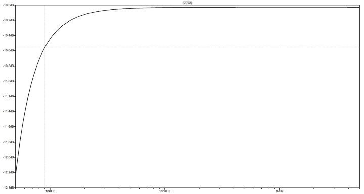
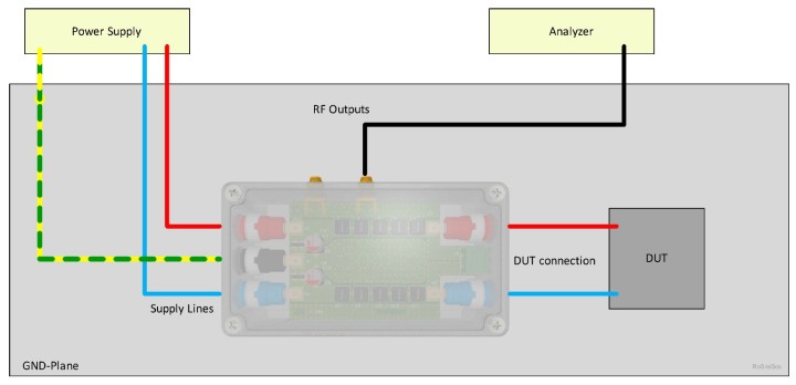
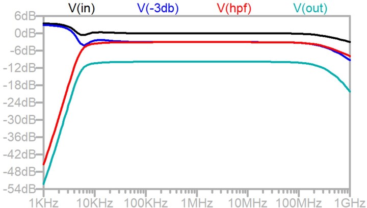
Simulation of signal path from DUT port to RF output (positive and negative) in frequency range of 5kHz – 5MHz
Simulation of signal path from DUT port to RF output (positive and negative) in frequency range of 1kHz – 1GHz. Marker from 9kHz – 200MHz attenuation -10 dB with max. tolerance -0,55 dB.
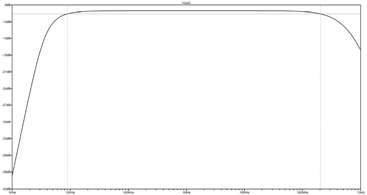
Impedance
 Impedance measurement of positive DUT port.
Description DC-LISN
The network simulation “dual DC LISN” is used to measure the conducted interference emissions of a test object in the frequency range of 150 kHz up to 200 MHz. The device based on the CISPR 25 / ISO 7637 standard for automotive electrical systems. It measures the RF interferences on both channels of such systems by using blocking inductance of 5µH. The design idea based on a demonstration circuit from Analog Devices (DC2130A – former Linear Technology).
The user will be able to measure differential mode as well as common mode noise.
Principe of noise decoupling
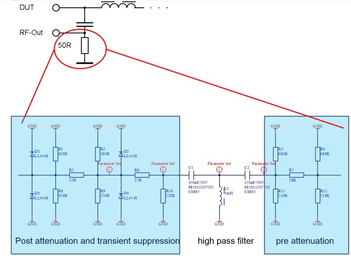
At a first step, the noise will see a PI-filter [V(-3db)] with -3dB to half the input power.
The next step is a third order high pass filter [V(hpf)] with a corner frequency of 5.5kHz (-3dB) to border the frequency range between 9kHz and around 200MHz (band pass functionality with parasitic capacitance from the diodes and inductor).
A last step brings the attenuation down to -10dB [V(out)]. This is a typical value for a LISN and must be corrected by the measurement equipment (e.g. internal 10dB gain or in Excel calculation).
The 5µH inductance should block the way back to the supply for the noise over the whole frequency range. 5µH typically used in CISPR25. If you use it for a CISPR22 setup, you should have a look to frequencies below around 400kHz. Because of the low inductance, there are lower levels you will measure.
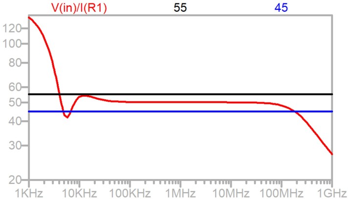
50 Ohm +/-10%: 45 Ohm @ 7kHz – 45 Ohm @ 185MHz
The decreasing impedance over 100MHz results in parasitic capacitance of the clamping diodes. These diodes are important to avoid high voltage spikes on the RF-outputs. If you use an oscilloscope with strong inputs, it would not be necessary!
Safety arrangement
In case of using this document and data to build this device for own usage, please keep in mind to save your own health.
- Read all documents
- Follow the safety instructions and warnings
- The device is only allowed to use for measurement applications that are specified. Other usage is forbidden.
Essential safety instructions
1. Please only use in inside rooms. For the power supply refer to the technical characteristics.
2. The product may only be used by authorized technical staff. The local or country-specific safety and accident prevention regulations must be observed for all work.
3. During operation of the product, function-related increased electromagnetic radiation and near fields can occur. Taking into account the increased need for protection of unborn life, pregnant women should be protected by suitable measures. People with pacemakers can also be at risk from electromagnetic radiation. The influence of electronic products outside of the operational EMC environment should be prevented by maintaining an appropriate safety distance or by using shielded rooms
4. Products / components must not be operated electrically, mechanically and / or thermally beyond their intended use.
5. To ensure proper operation, no changes may be made to the device.
6. Do not use the product under conditions in which condensation could or has occurred in or on the product, e.g. when the product has been moved from a cold to a warm environment.
7. Please only use neutral detergents for cleaning. Never use alcohol, benzene or thinner.
Technical characteristics
RF path
Channels: 2 (with clamping diodes)
Frequency range: 150 kHz – 200 MHz
Inductance: 5μH || 50 Ohm
Internal attenuation: 10 dB
DC path
Max. current: <10 ADC
Max. voltage: <60 VDC
DC resistance: <2x70mOhm
Size: 121mm x 66mm x 40mm (excluding connectors)
Test setup
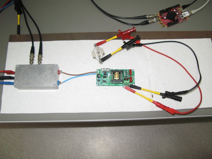
DUT is the prototype of the 12V-200V DC-DC converter for valve amplifiers (https://www.elektormagazine.com/labs/12v-200v-dc-dc-converter-for-valve-amplifiers)
Basic test setup which is still reasonably affordable: using a Red Pitaya STEMlab 125-14 with OS version 1.04-7. If the OS version is too old you may need to get the current OS from their website (https://www.redpitaya.com/n133/new-os-release-for-stemlab-and-sdrlab) and write it to the micro-SD card if the update manager is unable to connect. Use the application DFT Spectrum Analyser (yes, with an s). Downside of the STEMlab250-14 is a limited bandwidth of 62.5 MHz, but for most purposes this will be enough.

The vertical spectrum analyzer scale can only be set to dBm or dBu but not to dBµV, which is the preferred unit in various standards. It’s easy to convert dBm to dBµV: dBµV = dBm + 107 dB.
If you like multiple digits behind the decimal point: 1 mW in 50 Ω means a voltage of √(0.001 * 50) = 0.22361 V. So, the difference in dB to 1 µV is 20log(0.22361/(1*10-6)) = 106.9897 dB. Example: a level of -37 dBm is 70 dBµV. The data from the graph, a 1024-point FFT, can also be exported in CSV format. Import this data in Excel and there convert the data to dBµV and plot it in to a graph displaying a scale in dBµV. Then you can also place limit lines in the graph. See attachments for an example. As a precaution to protect the analyzer connect the analyzer only when the power supply connected to the LISN is turned on. Disconnect the analyzer from the LISN before turning off or unplugging the power source to the LISN. Terminate an unused output port with 50 Ω.
In case of conducted noise the cause for the interference voltage from 9 to 30 MHz is the ripple current on the input (differential mode) and interference currents through parasitic coupling to earth (common mode). Limits can be found in EN 61000-6-3. In product standard EN 55022, a derivative of CISPR 22, measurement methods are defined and limits specified. CISPR 22 has different values for Class A and Class B equipment and needs certification over the frequency range of 0.15 MHz to 30 MHz for conducted emissions.
CISPR 22 / EN 55022 conducted EMI limits
The standard divides equipment and devices intended to be used in the domestic environment in Class A and B. If Class B is not met and Class A is applied then following warning must be given:
Warning
This is a class A product. In a domestic environment this product may cause radio interference in which case the user may be required to take adequate measures.
Class A
Quasi-peak Average
(MHz) (dBµV) (dBµV)
0.15 - 0.50 79 66
0.50 - 30.0 73 60
Class B
Quasi-peak Average
(MHz) (dBµV) (dBµV)
0.15 - 0.50 66 to 56 56 to 46
0.50 - 5.00 56 46
5.00 - 30.0 60 50
For compliance all harmonics should stay below the average limits.
Another example
DUT:
“bad” sample
Summery of sub optimal placement and routing:
"good" sample

List of improvements:
Example for analyze measurements:
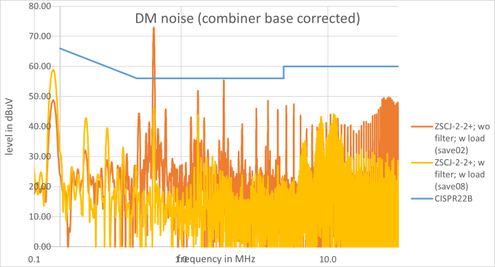
SMPS without filter, worse design and wrong component selection:

SMPS with filter, improved design and nice component selection:
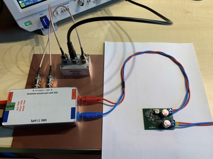
If we put the input of both devices to the LISN and the output to a load, we can measure the following DM and CM results.
Setup with combiner and worse design example.
DM part of both designs:
Soldering SMD components on the double sided 4 layerPCB
Reflow oven
Components on the top side, C5…C10 and L2…L11, can be soldered in a reflow oven. Soldering the inductors by hot air or a soldering iron with a fine tip will be difficult if not impossible because the pads of the inductors between them are almost inaccessible. Furthermore, the PCB is a 4-layer design and al lot of heat is needed to heat up a pad.
Hot air
Components on the bottom, like the small 0603 resistors, capacitors and two smaller inductors can be soldered using hot air. Usually a small 0603 resistor can be soldered by using a small soldering iron but a lot of heat flows into the 4 layers. When using hot air set the air flow to a minimum, otherwise these small components tend to drift.
The female SMA connectors (X1,X8) can be soldered with hot air. Put some solder paste on all pads on top and bottom of the first connector, slide the SMA onto the PCB and set the air flow higher to solder the connector on both sides. Solder the center pin first, then the ground contacts and then the ground contacts on the other side. Make sure the center pin is in the middle of the corresponding pad. Stop when all solder paste flows.
The spring contacts (contact fingers) can also be soldered using hot air and solder paste. Put some paste on the pads ((X13…X16) and put the contact upright. Stop when all solder paste flows and the contact clearly settles.
Soldering iron
The MiniMELFs can best be soldered with a soldering iron with a small chisel style tip (0.8..1 mm width is fine) and very thin solder, like 0.35 mm. First put some solder on a pad, preferably the ground pad because it will take a little while to get the solder to flow on these pads. Wait for this to happen and only then place the MiniMELF. The signal pad is easier to solder. Don’t use too much solder. Using tweezers, bring the MiniMELF to the correct spot on the PCB and solder one end. Look closely the diode is placed in the center of the designated area on the PCB. Of each pair of diodes of one the cathode (black ring) is soldered to ground and the anode of the other. Now solder the other end and solder the first solder joint again using a little extra solder. Always make sure not to use too much solder. Even better is to put some flux on the first pad before soldering. Remove the residual flux afterwards.
Once all parts are soldered onto the PCB on both sides, fasten the banana sockets to enclosure with the contacts turned vertically. Slide the PCB into the enclosure, SMA sockets into the corresponding holes and be careful the spring contacts on the bottom of the PCB are not bend by the edge of the enclosure.
Put some pressure on the PCB and place the washer (locking ring) and nut onto the SMA connectors. Then solder the contacts of the banana connectors to the pads (X2,X3,X5,X6,X7) while still keeping the PCB down a bit. Put the lid on the enclosure and the LISN is ready for use.
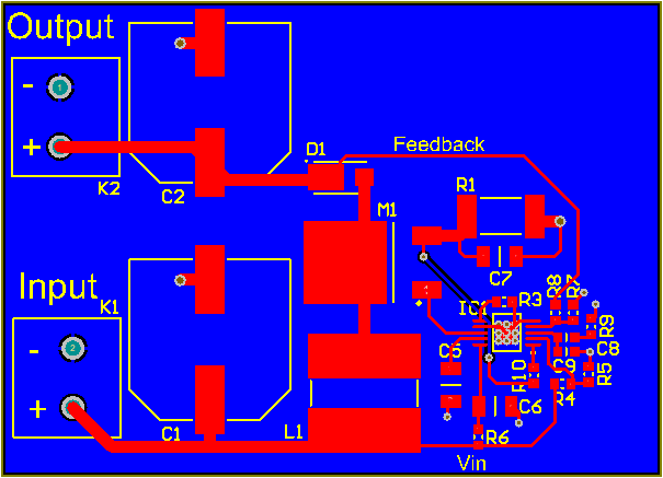
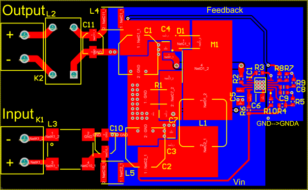
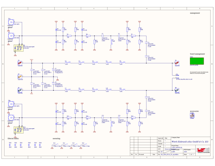
Schematic of the Dual DC LISN
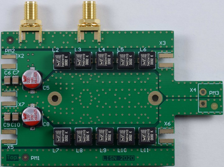
Top view of mounted PCB
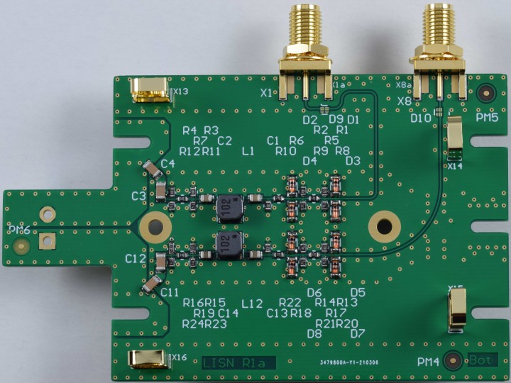
Bottom view of mounted PCB
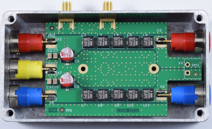
PCB placed inside the enclosure
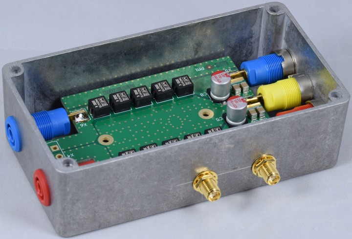
PCB placed inside the enclosure, side view on SMA connectors
Bill of materials (210296-1 v1.0)
Resistor (all SMD 0603)
R1, R13 = 820 Ω 1%
R2, R14 = 180 1%
R3, R4, R15, R16 = 680 Ω 1%
R5, R17 = 12 Ω 1%
R6, R18 = 27 Ω 1%
R7, R19 = 18 Ω 1%
R8, R20 = 910 Ω 1%
R9, R21 = 270 Ω 1%
R10, R22 = 220 Ω 1%
R11, R12, R23, R24 = 510 Ω 1%
Capacitor
C1, C2, C13, C14 = 470 nF 50 V SMD 0805 X7R (Würth Elektronik 885012207102)
C3, C4, C11, C12 = 100 nF 250 V SMD 1206 X7R (Würth Elektronik 885342208004)
C5, C8 = 22 uF 100 V SMD WCAP-ASLL (8x10.5) (Würth Elektronik 865060853003 or 865080853006)
C6, C7, C9, C10 = 2.2 uF 100 V SMD 1210 X7R (Würth Elektronik 885012209071)
Inductor
L1, L12 = 1 mH 200 mA SMD WE-LQS 5040 (Würth Elektronik 74404054102)
L2, L3, L4, L5, L6, L7, L8, L9, L10, L11 = 1.1 uH 15000 mA SMD WE-HCI 7050 (Würth Elektronik 744314110)
Semiconductor
D1, D2, D3, D4, D5, D6, D7, D8 = LL4148 100 V 100 mA, SMD MiniMelf (SOD-80)
D9, D10 = TVS, diode, not used/mounted
Other
X1,X8 = female SMA 9.52, 5 pins 180° (end launch), PCB 1.6 mm (Würth Elektronik 60312242114510)
X2, X3 = safety socket, 4mm, jack, panel mount, 24 A, 1 kV, gold plated contacts, red (Staubli 23.3000-22)
X5, X6 = safety socket, 4mm, jack, panel mount, 24 A, 1 kV, gold plated contacts, blue (Staubli 23.3000-23)
X7 = safety socket, 4mm, jack, panel mount, 24 A, 1 kV, gold plated contacts, green/yellow (Staubli 23.3000-20)
X13, X14, X15, X16 = WE-SECF SMD EMI Contact Finger, 7x2.5x13mm (Würth Elektronik 331161702513)
X4 = not mounted
Case = 1590N1 diecast aluminium 121.1x66x35.3 mm Hammond MFG
Misc.
PCB 210296-1 v1.0
Optional (to connect the LISN to the STEMlab 250-14)
4 SMA male - BNC adapters when using 2 standard BNC cables or 2 SMA cables (male-male)
Links:
http://rfemcdevelopment.eu/en/en-55022-2010
https://www.xppower.com/resources/blog/en55032-replaces-en55022
https://www.rohde-schwarz.com/uk/applications/a-homemade-lisn-for-precompliance-conducted-emission-tests-on-dc-dc-power-supplies-application-card_56279-1010752.html
https://www.youtube.com/watch?v=28oDdL9RnWM
https://www.youtube.com/watch?v=QPJzp66Yvzs
https://download.tek.com/document/37A_60141_1_HR_Letter.pdf
https://redpitaya.readthedocs.io/en/latest/quickStart/quickStart.html
Simulation of signal path from DUT port to RF output (positive and negative) in frequency range of 1kHz – 1GHz. Marker from 9kHz – 200MHz attenuation -10 dB with max. tolerance -0,55 dB.
Impedance
Description DC-LISN
The network simulation “dual DC LISN” is used to measure the conducted interference emissions of a test object in the frequency range of 150 kHz up to 200 MHz. The device based on the CISPR 25 / ISO 7637 standard for automotive electrical systems. It measures the RF interferences on both channels of such systems by using blocking inductance of 5µH. The design idea based on a demonstration circuit from Analog Devices (DC2130A – former Linear Technology).
The user will be able to measure differential mode as well as common mode noise.
Principe of noise decoupling
At a first step, the noise will see a PI-filter [V(-3db)] with -3dB to half the input power.
The next step is a third order high pass filter [V(hpf)] with a corner frequency of 5.5kHz (-3dB) to border the frequency range between 9kHz and around 200MHz (band pass functionality with parasitic capacitance from the diodes and inductor).
A last step brings the attenuation down to -10dB [V(out)]. This is a typical value for a LISN and must be corrected by the measurement equipment (e.g. internal 10dB gain or in Excel calculation).
The 5µH inductance should block the way back to the supply for the noise over the whole frequency range. 5µH typically used in CISPR25. If you use it for a CISPR22 setup, you should have a look to frequencies below around 400kHz. Because of the low inductance, there are lower levels you will measure.
50 Ohm +/-10%: 45 Ohm @ 7kHz – 45 Ohm @ 185MHz
The decreasing impedance over 100MHz results in parasitic capacitance of the clamping diodes. These diodes are important to avoid high voltage spikes on the RF-outputs. If you use an oscilloscope with strong inputs, it would not be necessary!
Safety arrangement
In case of using this document and data to build this device for own usage, please keep in mind to save your own health.
- Read all documents
- Follow the safety instructions and warnings
- The device is only allowed to use for measurement applications that are specified. Other usage is forbidden.
Essential safety instructions
1. Please only use in inside rooms. For the power supply refer to the technical characteristics.
2. The product may only be used by authorized technical staff. The local or country-specific safety and accident prevention regulations must be observed for all work.
3. During operation of the product, function-related increased electromagnetic radiation and near fields can occur. Taking into account the increased need for protection of unborn life, pregnant women should be protected by suitable measures. People with pacemakers can also be at risk from electromagnetic radiation. The influence of electronic products outside of the operational EMC environment should be prevented by maintaining an appropriate safety distance or by using shielded rooms
4. Products / components must not be operated electrically, mechanically and / or thermally beyond their intended use.
5. To ensure proper operation, no changes may be made to the device.
6. Do not use the product under conditions in which condensation could or has occurred in or on the product, e.g. when the product has been moved from a cold to a warm environment.
7. Please only use neutral detergents for cleaning. Never use alcohol, benzene or thinner.
Technical characteristics
RF path
Channels: 2 (with clamping diodes)
Frequency range: 150 kHz – 200 MHz
Inductance: 5μH || 50 Ohm
Internal attenuation: 10 dB
DC path
Max. current: <10 ADC
Max. voltage: <60 VDC
DC resistance: <2x70mOhm
Size: 121mm x 66mm x 40mm (excluding connectors)
Test setup
DUT is the prototype of the 12V-200V DC-DC converter for valve amplifiers (https://www.elektormagazine.com/labs/12v-200v-dc-dc-converter-for-valve-amplifiers)
Basic test setup which is still reasonably affordable: using a Red Pitaya STEMlab 125-14 with OS version 1.04-7. If the OS version is too old you may need to get the current OS from their website (https://www.redpitaya.com/n133/new-os-release-for-stemlab-and-sdrlab) and write it to the micro-SD card if the update manager is unable to connect. Use the application DFT Spectrum Analyser (yes, with an s). Downside of the STEMlab250-14 is a limited bandwidth of 62.5 MHz, but for most purposes this will be enough.
The vertical spectrum analyzer scale can only be set to dBm or dBu but not to dBµV, which is the preferred unit in various standards. It’s easy to convert dBm to dBµV: dBµV = dBm + 107 dB.
If you like multiple digits behind the decimal point: 1 mW in 50 Ω means a voltage of √(0.001 * 50) = 0.22361 V. So, the difference in dB to 1 µV is 20log(0.22361/(1*10-6)) = 106.9897 dB. Example: a level of -37 dBm is 70 dBµV. The data from the graph, a 1024-point FFT, can also be exported in CSV format. Import this data in Excel and there convert the data to dBµV and plot it in to a graph displaying a scale in dBµV. Then you can also place limit lines in the graph. See attachments for an example. As a precaution to protect the analyzer connect the analyzer only when the power supply connected to the LISN is turned on. Disconnect the analyzer from the LISN before turning off or unplugging the power source to the LISN. Terminate an unused output port with 50 Ω.
In case of conducted noise the cause for the interference voltage from 9 to 30 MHz is the ripple current on the input (differential mode) and interference currents through parasitic coupling to earth (common mode). Limits can be found in EN 61000-6-3. In product standard EN 55022, a derivative of CISPR 22, measurement methods are defined and limits specified. CISPR 22 has different values for Class A and Class B equipment and needs certification over the frequency range of 0.15 MHz to 30 MHz for conducted emissions.
CISPR 22 / EN 55022 conducted EMI limits
The standard divides equipment and devices intended to be used in the domestic environment in Class A and B. If Class B is not met and Class A is applied then following warning must be given:
Warning
This is a class A product. In a domestic environment this product may cause radio interference in which case the user may be required to take adequate measures.
Class A
Quasi-peak Average
(MHz) (dBµV) (dBµV)
0.15 - 0.50 79 66
0.50 - 30.0 73 60
Class B
Quasi-peak Average
(MHz) (dBµV) (dBµV)
0.15 - 0.50 66 to 56 56 to 46
0.50 - 5.00 56 46
5.00 - 30.0 60 50
For compliance all harmonics should stay below the average limits.
Another example
DUT:
“bad” sample
Summery of sub optimal placement and routing:
- Ground connection too far from the input/output capacitors (C1, C2), Mosfet Source / Rsens and IC Power GND à Large critical current loops
- Blocking capacitors C5 and C6 too far away from the IC and connected with too thin conductor tracks
- Feedback line comes from hard switching diode (D1). In addition, the feedback line should always be connected directly to the pad of the output capacitor (C2).
- Stub line (Vin) to input capacitor C1.
- AGND and PGND not separated
- Track to gate of mosfet (M1) to small
- Only one VIA at input/output capacitors GND connection
- Not optimal components for this kind of application (L1 unshielded, C1, C2 electrolytic caps with high ESR)
"good" sample
List of improvements:
- Feedback is connected after last output capacitor (C1)
- IC Vin connection comes from a silent point near C2
- Analog and Power GND merged in a quiet place
- The output is constructed with a common mode (L2) and a push-pull filter (L4, C11) and is able to filter broadband
- Blocking capacitors C5 & C6 very close to the IC pins
- Power loops connected over large and therefore very low inductive areas
- Critical loop around mosfet (M1), schottky diode (D1) and output capacitor (C4, C1) as small as possible (important for radiated emissions)
- Fully shielded choke (L1)
- Polymer electrolytic capacitors (C1, C2) supplemented by MLCCs (C3, C4) (even smaller ESR) to generate even less voltage ripples
Example for analyze measurements:
SMPS without filter, worse design and wrong component selection:
SMPS with filter, improved design and nice component selection:
If we put the input of both devices to the LISN and the output to a load, we can measure the following DM and CM results.
Setup with combiner and worse design example.
DM part of both designs:
Soldering SMD components on the double sided 4 layerPCB
Reflow oven
Components on the top side, C5…C10 and L2…L11, can be soldered in a reflow oven. Soldering the inductors by hot air or a soldering iron with a fine tip will be difficult if not impossible because the pads of the inductors between them are almost inaccessible. Furthermore, the PCB is a 4-layer design and al lot of heat is needed to heat up a pad.
Hot air
Components on the bottom, like the small 0603 resistors, capacitors and two smaller inductors can be soldered using hot air. Usually a small 0603 resistor can be soldered by using a small soldering iron but a lot of heat flows into the 4 layers. When using hot air set the air flow to a minimum, otherwise these small components tend to drift.
The female SMA connectors (X1,X8) can be soldered with hot air. Put some solder paste on all pads on top and bottom of the first connector, slide the SMA onto the PCB and set the air flow higher to solder the connector on both sides. Solder the center pin first, then the ground contacts and then the ground contacts on the other side. Make sure the center pin is in the middle of the corresponding pad. Stop when all solder paste flows.
The spring contacts (contact fingers) can also be soldered using hot air and solder paste. Put some paste on the pads ((X13…X16) and put the contact upright. Stop when all solder paste flows and the contact clearly settles.
Soldering iron
The MiniMELFs can best be soldered with a soldering iron with a small chisel style tip (0.8..1 mm width is fine) and very thin solder, like 0.35 mm. First put some solder on a pad, preferably the ground pad because it will take a little while to get the solder to flow on these pads. Wait for this to happen and only then place the MiniMELF. The signal pad is easier to solder. Don’t use too much solder. Using tweezers, bring the MiniMELF to the correct spot on the PCB and solder one end. Look closely the diode is placed in the center of the designated area on the PCB. Of each pair of diodes of one the cathode (black ring) is soldered to ground and the anode of the other. Now solder the other end and solder the first solder joint again using a little extra solder. Always make sure not to use too much solder. Even better is to put some flux on the first pad before soldering. Remove the residual flux afterwards.
Once all parts are soldered onto the PCB on both sides, fasten the banana sockets to enclosure with the contacts turned vertically. Slide the PCB into the enclosure, SMA sockets into the corresponding holes and be careful the spring contacts on the bottom of the PCB are not bend by the edge of the enclosure.
Put some pressure on the PCB and place the washer (locking ring) and nut onto the SMA connectors. Then solder the contacts of the banana connectors to the pads (X2,X3,X5,X6,X7) while still keeping the PCB down a bit. Put the lid on the enclosure and the LISN is ready for use.
Schematic of the Dual DC LISN
Top view of mounted PCB
Bottom view of mounted PCB
PCB placed inside the enclosure
PCB placed inside the enclosure, side view on SMA connectors
Bill of materials (210296-1 v1.0)
Resistor (all SMD 0603)
R1, R13 = 820 Ω 1%
R2, R14 = 180 1%
R3, R4, R15, R16 = 680 Ω 1%
R5, R17 = 12 Ω 1%
R6, R18 = 27 Ω 1%
R7, R19 = 18 Ω 1%
R8, R20 = 910 Ω 1%
R9, R21 = 270 Ω 1%
R10, R22 = 220 Ω 1%
R11, R12, R23, R24 = 510 Ω 1%
Capacitor
C1, C2, C13, C14 = 470 nF 50 V SMD 0805 X7R (Würth Elektronik 885012207102)
C3, C4, C11, C12 = 100 nF 250 V SMD 1206 X7R (Würth Elektronik 885342208004)
C5, C8 = 22 uF 100 V SMD WCAP-ASLL (8x10.5) (Würth Elektronik 865060853003 or 865080853006)
C6, C7, C9, C10 = 2.2 uF 100 V SMD 1210 X7R (Würth Elektronik 885012209071)
Inductor
L1, L12 = 1 mH 200 mA SMD WE-LQS 5040 (Würth Elektronik 74404054102)
L2, L3, L4, L5, L6, L7, L8, L9, L10, L11 = 1.1 uH 15000 mA SMD WE-HCI 7050 (Würth Elektronik 744314110)
Semiconductor
D1, D2, D3, D4, D5, D6, D7, D8 = LL4148 100 V 100 mA, SMD MiniMelf (SOD-80)
D9, D10 = TVS, diode, not used/mounted
Other
X1,X8 = female SMA 9.52, 5 pins 180° (end launch), PCB 1.6 mm (Würth Elektronik 60312242114510)
X2, X3 = safety socket, 4mm, jack, panel mount, 24 A, 1 kV, gold plated contacts, red (Staubli 23.3000-22)
X5, X6 = safety socket, 4mm, jack, panel mount, 24 A, 1 kV, gold plated contacts, blue (Staubli 23.3000-23)
X7 = safety socket, 4mm, jack, panel mount, 24 A, 1 kV, gold plated contacts, green/yellow (Staubli 23.3000-20)
X13, X14, X15, X16 = WE-SECF SMD EMI Contact Finger, 7x2.5x13mm (Würth Elektronik 331161702513)
X4 = not mounted
Case = 1590N1 diecast aluminium 121.1x66x35.3 mm Hammond MFG
Misc.
PCB 210296-1 v1.0
Optional (to connect the LISN to the STEMlab 250-14)
4 SMA male - BNC adapters when using 2 standard BNC cables or 2 SMA cables (male-male)
Links:
http://rfemcdevelopment.eu/en/en-55022-2010
https://www.xppower.com/resources/blog/en55032-replaces-en55022
https://www.rohde-schwarz.com/uk/applications/a-homemade-lisn-for-precompliance-conducted-emission-tests-on-dc-dc-power-supplies-application-card_56279-1010752.html
https://www.youtube.com/watch?v=28oDdL9RnWM
https://www.youtube.com/watch?v=QPJzp66Yvzs
https://download.tek.com/document/37A_60141_1_HR_Letter.pdf
https://redpitaya.readthedocs.io/en/latest/quickStart/quickStart.html
Diskussion (15 Kommentare)