


Automatic gain control with diode cascade
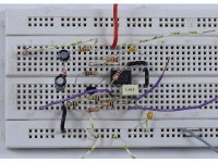
Automatically adjusts gain of small signals to keep the output level constant for a 35 dB range. Diode cascade is used to create the control voltage.
Using a JFET (T1, we used a J113 in a TO-92 package) as a variable resistor is nothing new and similar circuits have been published decades ago, probably since the first JFETs. Usually just one opamp is used and a single diode to rectify the output voltage. This DC voltage controls the Drain-Source resistance of the JFET. The higher the output voltage the higher this resistance. Since the JFET is part of the feedback this will establish a balance around the cut-off voltage of the JFET. Sadly, there are some issues that make the JFET not an ideal part for the job. For instance, the AC voltage across the Drain and Source causes a slight variation of the resistance and causes a fair degree of distortion. The higher this AC voltage the higher the distortion will be. A way to keep the signal across the JFET low is an application as a microphone amplifier for recording purposes or a bat detector perhaps. If a high gain is required (>1000) it’s best to use a second amplifier to keep the bandwidth of the entire circuit large enough, meaning larger than the standard audio bandwidth. At a unity-gain bandwidth of 3 MHz and a gain of 1500, bandwidth would be around 20 kHz and depends on the large tolerances of the opamp. In this example the maximum gain of the first opamp is maximal around 36 dB (63,5 x), but this depends on the minimum resistance of the JFET, here a J113. Part values and the dual-opamp used are all standard, except for the JFET. Schottky diodes are used for their low voltage drop and can be replaced by ordinary diodes, like a 1N4148. However, depending on the large voltage drop across the two diodes the nominal output level will be equally higher. The J113 can be replaced by other JFETs. Be aware connections and packages are not always the same. Even P-channel JFETs can be used. A positive gate voltage is needed then and the circuit must be modified by changing the rectifier, simply turn D1, D2, C2 and C3 around. A second issue is the large tolerance of the gate cut-off voltage of JFETs in general. Meaning the output level will depend on this specification. According to the datasheet the min and max value of a J111 are -3 V and 10 V respectively, for a J112 -1 V and -5 V, respectively and for a J113 -0.5 V and -3 V respectively. The J113 was chosen for its lowest maximum values. The nominal output voltage can vary between identical circuits. Since -3 V is still quite large a diode cascade, also called voltage multiplier, is used to create the gate voltage. This voltage is then almost equal to the peak to peak level of the output signal. Adding two extra diodes and capacitors will reduce the output level even more but also increase response (attack) time. This time can be made larger by increasing R7. But there is also a problem with the offset of the opamp. Any DC output voltage at the output of IC1A is amplified 22 times by IC1B. In our prototype the output voltage at the output of IC1B was maximal 0.5 V, hence the need for output decoupling capacitors C4 and C5 at the outputs. 0,5 V is too high and will also influence the nominal output level. The circuit can certainly benefit from a better contemporary opamp with much lower offsets. An AC coupling between IC1A and IC1B can make the loop become unstable. For experimentation a breadboard is ideal since components can be replaced without any effort. But maybe simulation is even faster, to see what changes to values and additions or omissions will have on the regulating loop (appearance of over and undershoot of the output level).
R1 defines the input impedance of 10 kΩ and C1 a low cut-off frequency of 16 Hz. The value of R2 plus the minimum resistance of T1 (UGS = 0, max. 100 Ω) sets the maximum gain. In our prototype this minimum value of T1 is lower, around 60 Ω (UGS = 0, measured with ohmmeter). So, the maximum gain for the total circuit is (1+R4/(R2+RDS))*(R6/R5) ≈ 1400 (if UGS = 0). R3 sets a minimum gain of IC1A in case the resistance of T1 is much higher than R3. But only when the input level is above a certain threshold where the circuit acts as a normal linear amplifier. In our prototype when the input level is above -24dBV (63 mV). R3 was omitted in the prototype, making the minimum gain of IC1A 1. Maximum input voltage just before clipping is about -15 dBV (178 mV) and is limited by the supply voltage of +/-9 V, chosen so two 9 V batteries can be used. R7 sets the attack time to milliseconds and can be increased. Do not reduce R7 because it will increase distortion at signal of K3 (but not K2) caused by the peak charging currents of C2 and C3. Recovery time is set by R8+R9, C2 and C3, a few seconds. Smaller values for C2 and C3 produce a higher ripple voltage and more distortion by the JFET. To reduce distortion a part of the voltage across the JFET is fed back to the gate. This reduces the gate voltage by half and the output level is twice as large as it would be if C3 was directly connected to the gate (only one 1 or 2 MΩ resistor parallel to ground then). Principle of the diode cascade is simple. A positive output voltage charges C2 through D1 and when the output goes negative C3 is charged by the output level of IC1B plus the voltage across C2 through D2 making the voltage of C3 almost the peak-peak value of the output signal at K3. By using this diode cascade the control voltage for the gate depends on both the positive and negative peak output level. Often the gate voltage is only created by only the positive part (P-channel JFET) or only the negative part (N-channel JFET) of the output voltage by using a single diode. The ripple frequency is however the same as with a single diode.
Measurements of the prototype (R3 omitted)
Power supply +/-9 V
Supply current 3,5 mA
Gain range K2 0…36 dB (1…63 x)
Gain range K3 36…63 dB (63…1397 x)
Low level bandwidth 16…55 kHz (at -60 dB input level, theor. 3 MHz/63.5 = 47 kHz)
High level bandwidth 16…≈ 200 kHz (at -15 dB input level)
Voltage C3 -1,9V (input level -60 dBV)
Voltage C3 -3,1 V (input level -25 dBV)
Maximum input level -15 dBV (178 mV, limited by supply voltage, no clipping at K3)
THD caused by T1, max. 0.84 % at -28 dBV input level (1 kHz, B = 22 kHz)
To give a better understanding what the circuit does two plots were recorded. The first shows input vs output level of K3 and shows an almost constant output level for a range of 35 dB at the input. The second one shows distortion vs input level at K3 for the same input level range as the first plot.
R1 defines the input impedance of 10 kΩ and C1 a low cut-off frequency of 16 Hz. The value of R2 plus the minimum resistance of T1 (UGS = 0, max. 100 Ω) sets the maximum gain. In our prototype this minimum value of T1 is lower, around 60 Ω (UGS = 0, measured with ohmmeter). So, the maximum gain for the total circuit is (1+R4/(R2+RDS))*(R6/R5) ≈ 1400 (if UGS = 0). R3 sets a minimum gain of IC1A in case the resistance of T1 is much higher than R3. But only when the input level is above a certain threshold where the circuit acts as a normal linear amplifier. In our prototype when the input level is above -24dBV (63 mV). R3 was omitted in the prototype, making the minimum gain of IC1A 1. Maximum input voltage just before clipping is about -15 dBV (178 mV) and is limited by the supply voltage of +/-9 V, chosen so two 9 V batteries can be used. R7 sets the attack time to milliseconds and can be increased. Do not reduce R7 because it will increase distortion at signal of K3 (but not K2) caused by the peak charging currents of C2 and C3. Recovery time is set by R8+R9, C2 and C3, a few seconds. Smaller values for C2 and C3 produce a higher ripple voltage and more distortion by the JFET. To reduce distortion a part of the voltage across the JFET is fed back to the gate. This reduces the gate voltage by half and the output level is twice as large as it would be if C3 was directly connected to the gate (only one 1 or 2 MΩ resistor parallel to ground then). Principle of the diode cascade is simple. A positive output voltage charges C2 through D1 and when the output goes negative C3 is charged by the output level of IC1B plus the voltage across C2 through D2 making the voltage of C3 almost the peak-peak value of the output signal at K3. By using this diode cascade the control voltage for the gate depends on both the positive and negative peak output level. Often the gate voltage is only created by only the positive part (P-channel JFET) or only the negative part (N-channel JFET) of the output voltage by using a single diode. The ripple frequency is however the same as with a single diode.
Measurements of the prototype (R3 omitted)
Power supply +/-9 V
Supply current 3,5 mA
Gain range K2 0…36 dB (1…63 x)
Gain range K3 36…63 dB (63…1397 x)
Low level bandwidth 16…55 kHz (at -60 dB input level, theor. 3 MHz/63.5 = 47 kHz)
High level bandwidth 16…≈ 200 kHz (at -15 dB input level)
Voltage C3 -1,9V (input level -60 dBV)
Voltage C3 -3,1 V (input level -25 dBV)
Maximum input level -15 dBV (178 mV, limited by supply voltage, no clipping at K3)
THD caused by T1, max. 0.84 % at -28 dBV input level (1 kHz, B = 22 kHz)
To give a better understanding what the circuit does two plots were recorded. The first shows input vs output level of K3 and shows an almost constant output level for a range of 35 dB at the input. The second one shows distortion vs input level at K3 for the same input level range as the first plot.
Want to build a project?
Bring your design to life with the Elektor PCB Service, powered by Eurocircuits. Upload the project files and order professionally manufactured PCBs or assembled boards through a proven European production platform.
Supporting KiCad, Eagle, Gerber, and ODB++ formats, the service is suitable for everything from prototypes and validation builds to series production and volume manufacturing.
Made in Europe. Fast. Reliable. Professional.
Diskussion (0 Kommentare)