
A nested number search
Pure digital electronics finds an imaginary number. I wanted to create a guessing game for my grandchild to get him used to larger numbers. A simple game idea emerged: Imagine a number in a given range of values. A display on a 7-segment-display prompts it to decide whether the imaginary number is greater than the number displayed or not. With these yes/no answers, the device finds the imaginary value after a certain number of questions.
The principle behind it is the interval nesting or in technical circles also called successive approximation, as is also used in AD converters.
It is no problem to solve this task with microcontroller systems. However, since I still have a lot of digital components, I decided to realize the game with pure digital electronics.
The principle
A simple branching tree for the number range 0 to 7 is shown in Fig. 1 to illustrate the interval nesting and the procedure. The number to be found is 5.
FIG.1
The first question asked is whether the number is greater than 3. This is answered with "yes" (step 1). Now you will be asked whether the number you are thinking of is greater than 5. This is not the case and the answer is no (Step 2). Now you will be asked if the number is greater than 4. This is answered with "yes" (step 3). The result is the number 5. With a total of three questions (steps) you can determine an imaginary number between 0 and 7.
Fig.2 shows the time sequence:
FIG.2
When starting in step 0, the "Event" register (event register) has the value "000". The 3 must be shown in the "Display".
The answer to step 1 is "yes". The event register is shifted one position to the left and the "1" is written as "yes" in the least significant position of the register -> "001". The 5 must be shown in the "Display". In step 2, the answer is "no". The event register is shifted one position to the left and the "0" is written as "no" in the least significant position of the register -> "010". The 4 must be shown in the "Display". In step 3, the answer is "yes". The event register is shifted one position to the left and the "1" is written as "yes" in the least significant position of the register -> "101". In the "Display" the 5 must be shown as the result.
For the number range from 0...7 with 3 questions (steps) it is not yet a problem to determine the appropriate display depending on the executed step and the content of the event register.
However, the circuit should cover the number range from 0...1023 with 10 questions (steps).
It is therefore essential to develop a mathematical algorithm. It is not necessary to study the formulas in detail as the resulting HEX file can be made available for programming the EPROM.
The formulas are listed in Fig.3:
FIG.3
"N" is the number of questions (steps).
"S" represents the step currently being executed.
"E" with index is the binary value of the event register bit whose position is defined by the index.
"A" is the calculated display value.
Three cases must be distinguished:
S=0:
For the above example in Fig.1, N=3.
This gives for A:
A=4-1=3
1<=S<=N-1
For the above example in Fig.1, N=3. For example, for step 2, the event register has the binary value 010. This results in A:
A=4-1-1+2=4
S=N
For the above example in Fig.1, N=3. For the last step 3, the event register has the binary value 101.
This gives for A:
A=1+0+4=5
So the formulas calculate the display A depending on N (number of questions), S (current step) and E (contents of the event register). With their help, you go through the branching tree step by step to the end result.
In the realized circuit, N=10. This means that a number range from 0 to 1023 can be queried with 10 questions.
The block diagram
The block diagram is shown in Fig.4:
FIG.4
The central component is the EPROM 32k x 8.
Its addresses A0 ... A3 are connected to the step counter "STEP" (binary 4-bit counter) and its addresses A4 ... A13 to the event register "EVENT" (10-bit shift register). The function of the remaining address A14 “MUX” will be described later.
The answered question is entered using the “YES” and “NO” buttons. As soon as one of the buttons is pressed, the step counter increments and the content of the event register is shifted one place to the left. If the "YES" button is pressed, a "1" is loaded into the first position of the event register; a "0" when the "NO" button is pressed.
Since the range of numbers should be 0 … 1023 (N=10), a total of four 7-segment displays must be controlled with the output data D0 … D7 of the EPROM. With a nibble (D0 ... D3 or D4 ... D7), one decimal place can be displayed via a BCD to 7-segment decoder. Two 7-segment displays can be controlled simultaneously with one data byte D0 ... D7. In order to enable four displays, it is necessary to switch back and forth between two displays each. Therefore, the 1s and 10s are in a group and the 100s and 1000s in combined a second group. Between these two groups, the oscillator is used to switch back and forth between the two groups. The EPROM is informed of which group is currently active via the signal MUX (A14).
The circuit
Fig.5 shows the circuit diagram
FIG.5
The answers are entered using the TA2 (NO) and TA3 (YES) keys. The clock signal CLK_C for the step counter IC5 is generated via the diodes D1 and D2, the debouncing and delay element R24, C11 and the NAND gates IC6C, IC6D and IC4D. The inverted clock signal CLK_S for the three cascaded 4-bit shift registers of the event register IC7A, B and IC8A is generated via the transistor stages T5, R22 and R27.
As already described in the block diagram, the outputs of the step counter and the event shift register are connected to the corresponding address inputs of the EPROM IC1. With the gate IC4B, when the step counter reading is 10, at which the result is fixed, the clock inputs CLK_C and CLK_S are blocked via the gate IC4D, so pressing a button has no effect.
In addition, when the count is 10, the oscillator IC4A, C5, R19 is activated via the gate IC4C. It is connected to the "blank inputs" of the two BCD to 7-segment decoders IC2, IC3 and causes the 7-segment displays DIS1 ... DIS4 to display the end result flashing.
As already described in the block diagram, the 7-segment displays are divided into the groups DIS1, DIS2 and DIS3, DIS4. Switching between the two groups takes place using driver stages T1, T2, R8, R17 or T3, T4, R9, R18 with the signals A_L or A_H, which are generated by the oscillator IC6A, IC6B, C8, R20. The signal A_H is connected to the address A14 of the EEPROM IC1 for switching between the two display groups.
When you press the TA1 "RES" button or turn the device on (C13), the game starts over.
The creation of the HEX file for the EPROM
The EPROM must be programmed in such a way that, depending on the value of addresses A0 ... A3 (step "S") and A4 ... A13 (event "E"), the correct display "A" occurs according to the algorithms shown in Fig.3. In addition, to display four 7-segment displays, the two display groups must be multiplexed (MUX) via A14. Display value A must be determined for each address in the complete EPROM address range from 0000h … 7FFFh. Addresses that do not make sense should be written with FFh. The problem can only be solved with a special program. For the sake of simplicity, BASCOM was chosen. It has the advantage that bit functions are easily possible. The program was run once on an ATMEGA8, and a LOG file was created and saved using the terminal with the simple PRINT command.
Fig.6 shows a small excerpt from the HEX file in the lowest address area
FIG.6
Interpretation example:
In the implemented circuit, N=10. The first display at address 0000h must therefore be 511 (see Fig.3, S=0). Since only the 1s and 10s are represented under this address (A14=0), the first byte must be 11h. If the first question (step 1) is answered with "NO", the first bit of the event register remains 0; the step counter increments to 1. The address is therefore 0001h, the display must be 255 (see Fig.3, 1<=S<=N-1). Here, too, only the 1s and 10s are shown with 55h. Incidentally, an Fh means that the corresponding 7-segment display is dark.
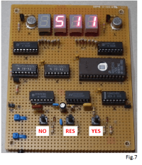
The prototype
Fig.7 shows the functional model directly after switching on. It was realized using the threading technique. The +5V power supply is provided via a USB connection cable.
FIG.7
If you are interested in duplicating the circuit, a circuit board layout can be created.
The BASCOM program to create the HEX-File, the HEX file generated or the programed EEPROM can be made available.
It is no problem to solve this task with microcontroller systems. However, since I still have a lot of digital components, I decided to realize the game with pure digital electronics.
The principle
A simple branching tree for the number range 0 to 7 is shown in Fig. 1 to illustrate the interval nesting and the procedure. The number to be found is 5.
FIG.1
The first question asked is whether the number is greater than 3. This is answered with "yes" (step 1). Now you will be asked whether the number you are thinking of is greater than 5. This is not the case and the answer is no (Step 2). Now you will be asked if the number is greater than 4. This is answered with "yes" (step 3). The result is the number 5. With a total of three questions (steps) you can determine an imaginary number between 0 and 7.
Fig.2 shows the time sequence:
FIG.2
When starting in step 0, the "Event" register (event register) has the value "000". The 3 must be shown in the "Display".
The answer to step 1 is "yes". The event register is shifted one position to the left and the "1" is written as "yes" in the least significant position of the register -> "001". The 5 must be shown in the "Display". In step 2, the answer is "no". The event register is shifted one position to the left and the "0" is written as "no" in the least significant position of the register -> "010". The 4 must be shown in the "Display". In step 3, the answer is "yes". The event register is shifted one position to the left and the "1" is written as "yes" in the least significant position of the register -> "101". In the "Display" the 5 must be shown as the result.
For the number range from 0...7 with 3 questions (steps) it is not yet a problem to determine the appropriate display depending on the executed step and the content of the event register.
However, the circuit should cover the number range from 0...1023 with 10 questions (steps).
It is therefore essential to develop a mathematical algorithm. It is not necessary to study the formulas in detail as the resulting HEX file can be made available for programming the EPROM.
The formulas are listed in Fig.3:
FIG.3
"N" is the number of questions (steps).
"S" represents the step currently being executed.
"E" with index is the binary value of the event register bit whose position is defined by the index.
"A" is the calculated display value.
Three cases must be distinguished:
S=0:
For the above example in Fig.1, N=3.
This gives for A:
A=4-1=3
1<=S<=N-1
For the above example in Fig.1, N=3. For example, for step 2, the event register has the binary value 010. This results in A:
A=4-1-1+2=4
S=N
For the above example in Fig.1, N=3. For the last step 3, the event register has the binary value 101.
This gives for A:
A=1+0+4=5
So the formulas calculate the display A depending on N (number of questions), S (current step) and E (contents of the event register). With their help, you go through the branching tree step by step to the end result.
In the realized circuit, N=10. This means that a number range from 0 to 1023 can be queried with 10 questions.
The block diagram
The block diagram is shown in Fig.4:
FIG.4
The central component is the EPROM 32k x 8.
Its addresses A0 ... A3 are connected to the step counter "STEP" (binary 4-bit counter) and its addresses A4 ... A13 to the event register "EVENT" (10-bit shift register). The function of the remaining address A14 “MUX” will be described later.
The answered question is entered using the “YES” and “NO” buttons. As soon as one of the buttons is pressed, the step counter increments and the content of the event register is shifted one place to the left. If the "YES" button is pressed, a "1" is loaded into the first position of the event register; a "0" when the "NO" button is pressed.
Since the range of numbers should be 0 … 1023 (N=10), a total of four 7-segment displays must be controlled with the output data D0 … D7 of the EPROM. With a nibble (D0 ... D3 or D4 ... D7), one decimal place can be displayed via a BCD to 7-segment decoder. Two 7-segment displays can be controlled simultaneously with one data byte D0 ... D7. In order to enable four displays, it is necessary to switch back and forth between two displays each. Therefore, the 1s and 10s are in a group and the 100s and 1000s in combined a second group. Between these two groups, the oscillator is used to switch back and forth between the two groups. The EPROM is informed of which group is currently active via the signal MUX (A14).
The circuit
Fig.5 shows the circuit diagram
FIG.5
The answers are entered using the TA2 (NO) and TA3 (YES) keys. The clock signal CLK_C for the step counter IC5 is generated via the diodes D1 and D2, the debouncing and delay element R24, C11 and the NAND gates IC6C, IC6D and IC4D. The inverted clock signal CLK_S for the three cascaded 4-bit shift registers of the event register IC7A, B and IC8A is generated via the transistor stages T5, R22 and R27.
As already described in the block diagram, the outputs of the step counter and the event shift register are connected to the corresponding address inputs of the EPROM IC1. With the gate IC4B, when the step counter reading is 10, at which the result is fixed, the clock inputs CLK_C and CLK_S are blocked via the gate IC4D, so pressing a button has no effect.
In addition, when the count is 10, the oscillator IC4A, C5, R19 is activated via the gate IC4C. It is connected to the "blank inputs" of the two BCD to 7-segment decoders IC2, IC3 and causes the 7-segment displays DIS1 ... DIS4 to display the end result flashing.
As already described in the block diagram, the 7-segment displays are divided into the groups DIS1, DIS2 and DIS3, DIS4. Switching between the two groups takes place using driver stages T1, T2, R8, R17 or T3, T4, R9, R18 with the signals A_L or A_H, which are generated by the oscillator IC6A, IC6B, C8, R20. The signal A_H is connected to the address A14 of the EEPROM IC1 for switching between the two display groups.
When you press the TA1 "RES" button or turn the device on (C13), the game starts over.
The creation of the HEX file for the EPROM
The EPROM must be programmed in such a way that, depending on the value of addresses A0 ... A3 (step "S") and A4 ... A13 (event "E"), the correct display "A" occurs according to the algorithms shown in Fig.3. In addition, to display four 7-segment displays, the two display groups must be multiplexed (MUX) via A14. Display value A must be determined for each address in the complete EPROM address range from 0000h … 7FFFh. Addresses that do not make sense should be written with FFh. The problem can only be solved with a special program. For the sake of simplicity, BASCOM was chosen. It has the advantage that bit functions are easily possible. The program was run once on an ATMEGA8, and a LOG file was created and saved using the terminal with the simple PRINT command.
Fig.6 shows a small excerpt from the HEX file in the lowest address area
FIG.6
Interpretation example:
In the implemented circuit, N=10. The first display at address 0000h must therefore be 511 (see Fig.3, S=0). Since only the 1s and 10s are represented under this address (A14=0), the first byte must be 11h. If the first question (step 1) is answered with "NO", the first bit of the event register remains 0; the step counter increments to 1. The address is therefore 0001h, the display must be 255 (see Fig.3, 1<=S<=N-1). Here, too, only the 1s and 10s are shown with 55h. Incidentally, an Fh means that the corresponding 7-segment display is dark.
The prototype
Fig.7 shows the functional model directly after switching on. It was realized using the threading technique. The +5V power supply is provided via a USB connection cable.
FIG.7
If you are interested in duplicating the circuit, a circuit board layout can be created.
The BASCOM program to create the HEX-File, the HEX file generated or the programed EEPROM can be made available.
Updates des Autors