
433-MHz Modules for Telemetry and more [130023-I]
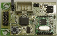
from the lab (1-8-2013)We changed a few things to the original design. We removed the RS232 connecter and with it a MAX232A. In its place we added our Embedded Communication Connector (ECC), as a gateway module.
from the lab (1-8-2013)
We changed a few things to the original design. We removed the RS232 connecter and with it a MAX232A. In its place we added our Embedded Communication Connector (ECC), as a gateway module. Our USB-FT232R breakout-board (110553-91) can be connected to this connector (to pins 2/4/6/8), giving it a USB connection (Photo2_USB-FT232R breakout-board.jpg). The processor was replaced by one of the same family but with more memory, the ATmega328P. All data lines to the 433 MHz module are connected to the processor, (including nINT/VDI). We added a push button and a led (D1). Led D2 is a power indicator. A pull-up resistor is connected to nSEL to prevent a programmer sending commands to the RFM12B. Jumper JP1 gives a choice to use a separate power supply for this circuit or use the power available on the ECC. In case an external power supply is used a 5 V regulator (IC2) is present. The input voltage may vary between 6 and 12 V. The regulator is cooled by copper planes on the PCB. Schottky diode D3 is to prevent damage to the circuit in case the external power supply is connected the wrong way round.
Problem is that the original 5 V version of the RFM12 is hard to find. We used a 3.3 V version instead (RFM12B). The processor won’t run on 16 MHz if its power supply is 3.3V (maybe 12 MHz max.). So we decided to make a little adapter to be placed between the RF module and the PCB. The adapter consists of 8 resistor dividers and a 3.3 V regulator. This little PCB (130023-2) is only 16.8 by 19.6 mm (Photo3_adapter_130023-2.jpg). To connect the RF module to the adapter two additional 2 mm pin headers (SIL-7) are required. We use one 14 pin version that can easily be broken in two halves. Dividers R1/R2 through R15/R16 reduce the 5 V levels to just under 3.3 V. The output signals from the RFM12 to the processor are high enough for the processor to accept without errors. Since the RFM12B only draws a few mA (26 mA max. for the 433 MHz band) this voltage regulator can be very small. We chose one in a SOT-23 case. This little regulator can supply 150 mA at 1.7 V between in and output, more than enough for our purpose. For testing purposes we used additional sockets. This makes the removal of the adapter and module easy (Photo4_adapter+sockets.jpg). We don’t mention them in the BOM because the ones we found are too expensive.
Our test setup uses a notebook and a PC. We programmed one prototype as transmitter and another one as receiver, using the software the author supplied. Connected to the ECC of each prototype is a USB-FT232R breakout-board (110553-91). One is connected to the notebook and the other one to the PC. Both are using HTerm as a terminal program. This setup works but there are several issues that need to be addressed. For instance after power-up the RFM12B transmits a carrier wave continuously. Only after transmitting ends the carrier is switched off reducing power consumption by a factor two. If one circuit is programmed as a receiver there is no protection against suppressing noise and disturbances, which is simply being forwarded as data. The present firmware versions do not support bidirectional communication. At this point the firmware needs upgrading.
Designs version 1.2 of 130023-1 and version 1.0 of 130023-2 are working well. Here are the BOMs.
Bill of materials 130023-1 PCB v1.2
Resistor
R1,R4 = 1 kΩ, 5 %, 125 mW, SMD 0805
R2,R3 = 10 kΩ, 5 %, 125 mW, SMD 0805
Capacitor
C1,C2 = 22 pF, 5 %, 50 V, CG0/NP0, SMD 0805
C3-C7 = 100 nF, 10 %, 50 V, X7R, SMD 0805
C8 = 4.7 µF, 10 %, 6.3 V, X5R, SMD 0805
C9 = 10 µF, -20/+80 %, 25 V, Y5V, SMD 1206
Semiconductor
D1 = LED Green, SMD 0805
D2 = LED Red, SMD 0805
D3 = PMEG2010AEH, 1A, 20 V, SMD SOD-123F
IC1 = ATmega328P-AU, SMD TQFP-32
IC2 = NCP5501DT50G, SMD DPAK-3
Other
K1 = Header straight, 2x5, 2.54 mm spacing
K2 = Header straight, 2x3, 2.54 mm spacing
K3 = 2-way pinheader SIL, 2.54 mm spacing
JP1 = 3-way pinheader SIL, 2.54 mm spacing
JP1 = Jumper 2.54 mm
S1 = Switch tactile 6x6 mm SPST-NO, 12 V 50 mA
X1 = Crystal, 16 MHz, 50 ppm, Cload 18 pF, 5x3.2 mm, SMD ABM3, Abracon ABM3-16.000MHZ-B2-T
MOD1 = RF module, transceiver, FSK, 433 MHz, 3.3 V, Hope Microelectronics co., Ltd RFM12B-433-S1
MOD1 = Header straight, SIL 14way, 2 mm spacing
Misc.
PCB 130023-1 v1.2
Bill of materials 130023-2 PCB v1.0
Resistor
R1,R3,R5,R7,R9,R11,R13,R15 = 1k8, 5 %, 100 mW, SMD 0603
R2,R4,R6,R8,R10,R12,R14,R16 = 3k3, 1 %, 100 mW, SMD 0603
Capacitor
C1,C2 = 1 µF, 20 %, 6V3, SMD 0603, X5R
Semiconductor
IC1 = XC6206P332MR
Other
MOD1 = Header straight, SIL 14way, 2 mm spacing
Misc.
PCB 130023-2 v1.0
author: Günter Gerold [tv@gerold-online.de ]
Jens post de software nog (26-2-2013)
Sender:
Damit ein Streaming über die RFM12 möglich ist, muss die Baudrate der Funkstrecke höher sein, als die Baudrate der zugeführten Daten. Für eine hohe Baudrate der Funkstrecke ist es wiederum wichtig, dass die Daten schnell genug in das RFM12 Modul gelangen. Deshalb ist der erste Schritt die Geschwindigkeit der SPI-Verbindung zwischen ATMega88 und RFM12-Modul festzulegen. Im Datasheet des SI4420 steht in einem Nebensatz, dass die höchste Datenrate beim 10MHz Quarz des RFM12 2,5MHz beträgt. Mit den Teilern der SPI-Register wird im ATMega deshalb ein Takt von 2MHz eingestellt.
'SPI einrichten, Master 2MHz bei 16MHz (max. 2,5MHz erlaubt)
SPCR = &B01010001
SPSR = 1
SPCR = &B01010001
SPSR = 1
Die Register des SI4420 bestehen aus 16 Bit, die Hardware-SPI sendet aber immer nur 8 Bit. Somit müssen 2 Byte gesendet werden um ein Register zu setzen. Um festzustellen ob die Übertragung tatsächlich funktioniert, kann der CLK-Ausgang des RFM12 Moduls genutzt werden. Mit dem Register 82xxh kann mit dem Bit0 der CLK-Ausgang ein und ausgeschaltet werden. Wird 8200h übertragen sollte am CLK-Pin ein 10MHz Sinus zu messen sein. Nach Übertragung von 8201h sollte der Sinus verschwunden sein.
Nachdem die Register laut Datasheet gesetzt sind, geht’s ans Senden. Ein Sendeblock besteht aus einer Preamble, ein oder zwei Bytes Synchron Pattern und den eigentlichen Daten. Die Preamble besteht aus zwei Bytes mit dem Wert AAh = 10101010 binär. Die abwechselnden Nullen und Einsen helfen dem Empfänger beim Synchronisieren mit dem Sender. Die folgenden beiden Bytes 2Dh und D4h signalisieren dem Empfänger, dass jetzt Daten folgen.
Theoretisch könnte man jetzt endlos Daten schicken, jedoch kann eine kurze Störung das ganze Datenpaket nutzlos machen. Ebenso unklug ist es jedes Byte einzeln zu verschicken, da der Overhead den Datendurchsatz stark herabsetzt. Darum werden die Datenpakete mit einem Stoppbyte abgeschlossen und die Funkübertragung beendet. Als Stoppbyte ist der Wert 10 (Ascii LF) festgelegt. Zusätzlich könnte die Anzahl der gesendeten Bytes mitgeschickt werden, auch eine Redundanzprüfung (CRC) ist denkbar.
Manche werden sich wundern, warum im Code der Wert AAh nur nach der Datenübertragung zu finden ist und nicht davor. Der Grund ist wieder im Datasheet zu finden. Mit dem Setzen des EL-Bits vor Beginn der Datenübertragung wird der zwei Byte große Sendepuffer mit AAAAh vorbelegt. Wird nun der Sender eingeschaltet, verlässt das erste Byte sofort den Sender. Danach meldet der PIN SDO den Erfolg und das erste Datenbyte wird in den Sendepuffer geschrieben. Währenddessen verlässt das zweite AAh den Sender usw. Das letzte Datenbyte würde aber im Sendepuffer stehenbleiben, weshalb ein Dummybyte nachgeschoben wird. Der Wert dieses Bytes ist egal.
Nachdem der Datenblock jetzt erfolgreich gesendet ist, wartet der ausgeschaltete Funksender auf das nächste Datenpaket. Damit sich die UART und die SPI-Übertragung nicht in die Quere kommen ist der Datenpuffer in zwei Bereiche geteilt:
Dim RXBuf(80) as byte
'Startpunkt unterer String
const startbyteA = 1
'Startpunkt oberer String
const StartbyteB = 40
'aktueller Startpunkt des Strings fürs Senden
dim von as byte
'aktuelles Ende des Strings fürs Senden
dim bis as byte
'Startpunkt unterer String
const startbyteA = 1
'Startpunkt oberer String
const StartbyteB = 40
'aktueller Startpunkt des Strings fürs Senden
dim von as byte
'aktuelles Ende des Strings fürs Senden
dim bis as byte
Das kann man sich als eine Art Ringspeicher vorstellen. Während die UART die eine Hälfte beschreibt, liest das SPI die andere Hälfte aus. Der Datenempfang der UART ist Interrupt gesteuert. Ist ein Byte komplett empfangen wird ein Interrupt ausgelöst, welcher das Byte sofort wegspeichert. Wichtig ist hier, dass die Interrupt Routine so kurz wie möglich ist, denn bis zum nächsten UART-Byte will ja auch noch das RFM12 gefüttert werden.
Empfänger:
Beim Empfänger müssen nun auch Daten vom RFM12 Modul gelesen werden. Auch hier gibt es die Möglichkeit festzustellen ob die Datenübertragung mit SPI funktioniert. Wird der Pin nInt auf Masse gezogen wird im Statusregister das dazugehörige Flag EXT gesetzt.
Am Pin FFIT des RFM12-Moduls wird durch High-Pegel signalisiert, dass im Empfangspuffer ein Byte angekommen ist. Dieses wird sofort an die UART weitergegeben. Hat das Byte den Wert des Schlussbytes, wird das FIFO-Register initialisiert. Nun wird wieder auf ein Synchronpattern gewartet.
Diskussion (0 Kommentare)