
2nd Order Adjustable Treble Boost [230190]
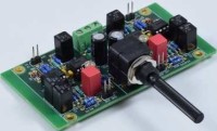
High quality circuit for amplifying the highest audio frequencies as a correction for getting older. The circuit needs a +/-12 V power supply. The 100 mm wide PCB fits in 1455 Hammond enclosures.
Getting older often means hearing high frequencies less good. The intent of this circuit is to compensate this by using a steeper correction starting at a higher frequency than a standard Baxandall tone control, usually working around 1 kHz. Of coarse where exactly the correction should start is very personal. With the values here the operating point (start of increase of the gain) shifts from approximately 6 to 3 kHz, depending of the gain setting of the potentiometer. The higher the gain the sooner the correction starts. Maximum amplification is 12 dB (4 x) at 17 kHz (P1 in maximum position). The bandwidth of the output stage is limited to 48 kHz to prevent amplification of frequencies far outside the human hearing range and thus reduce the susceptibility of the circuit for high frequency interferences.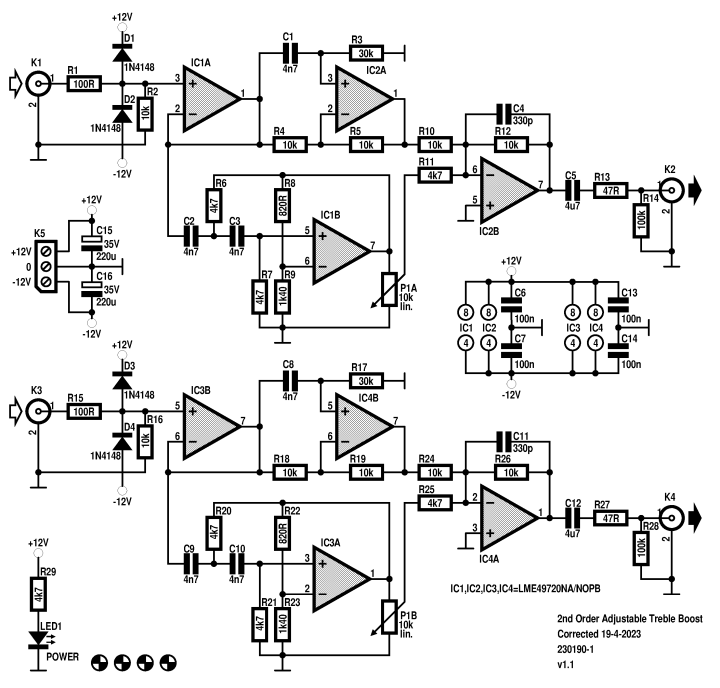
The principle of the circuit is simple, sum the output of a 2nd order highpass filter and it’s input signal. Just adding the two signals will have an unwanted effect on the desired summation caused by the phase change of the filter. To correct this the input signal of filter IC1B is corrected by allpass filter IC2A before summation with its output signal, by summing amplifier IC2B, otherwise some frequencies can get attenuated. A second order critically damped filter has the same phase change as an allpass filter. However the slope of this type of filter is not as steep as desired. Using a Butterworth filter instead causes the phase change to be different and the allpass can’t quite correct this steeper filter. This results in a small variance of the gain at lower frequencies, less then +0.2 dB around 900 Hz and -0.3 dB around 3 kHz, depending on the exact operating point of the allpas filter. To make the highpass and allpass filter independent of the impedance of the source signal voltage follower IC1A is added at the input. D1, D2 and R1 protect the input of the opamp against possible overvoltage and spikes. Input impedance is mainly defined by R2, so 10 kΩ. The output signal of the allpass filter is directly connected to the summing amplifier. The gain is defined by the ratio of R12 and R10, so unity gain. The gain of output signal of the highpass filter is set by the ratio of R12 and R11.
To make it easier to change the frequency at which the treble boost starts, should anyone require a different correction, the Butterworth filter also has a small gain of 1,5857 x. At the theoretical gain of 3 - √2 (= 1.5858) the resistors and capacitors have the same values, so C2 = C3 and R6 = R7. If a change is needed the circuit is simple enough to simulate it as a way to find out what the change of component values has on the characteristic of the treble boost. Capacitor C1 has the same value as C2 and C3 and make it easy to change the operating point, all 3 capacitors should have the same value. Of course changing R3 and R6 and R7 proportionately is also an option. The value of 4.7 nF (C1/C2/C3) is chosen because it is available as 1 % polystyrene capacitor and this dielectric is an excellent choice to guarantee low tolerance and low distortion. Also the reason why C4 is a 1 % polystyrene capacitor (axial, placed upright). The low tolerance of all filter components make the phase change between the two chancels as low as possible. A cheaper solution but much lower quality and higher tolerance is the use of standard 5 mm PET capacitors for C1…C3/C8…C10 and 5 mm ceramic (use at least NP0/C0G dielectric) for C4 and C11.
To have a total gain of 12 dB (4x) around 17 kHz the gain of the highpass filter and the small attenuation caused by the bandwidth limiting capacitor C4 also have to be taken into account, in addition to the ratio of R12/R11. Total gain should be 3 to get 4 times the input signal at the output of the summing amplifier. Without C4 maximum gain of the highest frequencies would be 3,37: (1+820 Ω/1.4 kΩ)*(10 kΩ/4.7 kΩ).
Although a quad opamp could have been used for each channel, the amount of high quality dual opamps is far greater and some have much better properties. An excellent choice is the LME49720 which is also (still) available in an 8 pins DIP package. Its high Gain Bandwidth Product of 55 MHz and extreme low distortion of less than 0.00007 % at 20 kHz in a 2 kΩ load (3 VRMS , +/-12 V) make it an excellent choice for this type of circuit. It also has a very low input offset voltage. Offset at the output of the summing amplifiers varies slightly with the position of P1 but stayed below 1 mV in the prototype. Should another opamp be used the offset can be much higher. Capacitor C5 blocks any DC voltage at the output. The cutoff frequency with a 10 kΩ load is 3.7 Hz.
Total quiescent current of the prototype is +44.7/-42.6 mA. The current through LED1 is 2.1 mA. The quiescent current of a LME49720 is typically rated 10 mA at +/-15 V. To use a standard AC adapter as power supply a DC-DC converter is one way of creating a symmetrical power supply for the treble boost. Total power of the circuit is 1.05 W, so a 1 W DC-DC converter should probably be sufficient, but one with a slightly higher power output is advisable. Use one with regulated outputs. Most symmetrical DC-DC converter series have an output voltage of +/-12 V, the reason why +/-12 V is chosen as the power supply voltage. However, power supply voltage range of the LME49720 is +/-2.5 to +/-17 V.
The width of the PCB is extended to almost 100 mm so it can fit in the 1455 series of Hammond enclosures. The PCB can be shortened to the white lines. 4 mounting hole can be used to fasten the PCB in any other enclosure. Enclosure 1455N1201 would be a nice choice. However, the potentiometer is about 1 mm too high if the PCB is placed in the lowest slots. Bending the wider part of the leads of the potentiometer slightly towards the body can make the potentiometer low enough to make it fit. Just a thought. Another option is placing the potentiometer with its thread through the front (of any enclosure) and use short thin flexible wires to connect it to the PCB. This way any linear dual gang 10 kΩ potentiometer can be used.
Warning: as with all treble controls at high volume settings and maximum treble boost the power output of a power amplifier to a tweeter can be too much and damage it! An increase of 4 times in amplitude means 16 times an increase in power!
Measurements prototype
Vin max (1 kHz, THD = 0.1 %) 7.9 V
Quiescent current (Vs +/-12 V) +44.7/-42.6 mA
Bandwidth (P1 min.) 3.7 Hz…48 kHz (load 10 kΩ)
Max. Gain @ 17 kHz (P1 max.) 12 dB
THD+N (1 kHz, 1 V, P1 min.) 0.0008 % (B= 22 kHz)
THD+N (1 kHz, 1 V, P1 max.) 0.0012 % (B = 22 kHz)
THD+N (1 kHz, 1 V, P1 min.) 0.0012 % (B = 80 kHz)
THD+N (1 kHz, 1 V, P1 max.) 0.0016 % (B = 80 kHz)
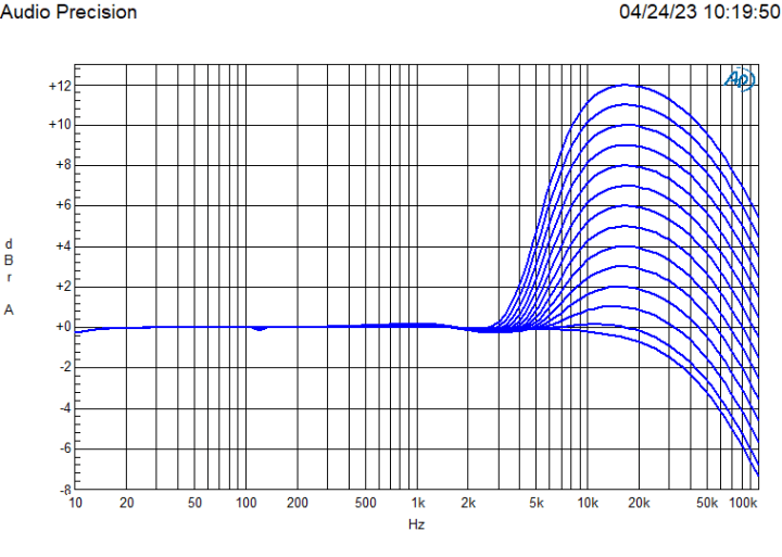
Plot A shows the amplitude from 10 to 100 kHz and gives a good impression of the characteristic of this adjustable treble boost. P1 is adjusted to have 1 dB steps at 17 kHz. In the lowest but one plot P1 is adjusted to 0 dB gain at 17 KHz. For the lowest plot P1 is set to its minimum position. Depending on the setting of P1 the operating point shifts from approximately 6 kHz to 3 kHz when P1 is adjusted from minimum to maximum setting.
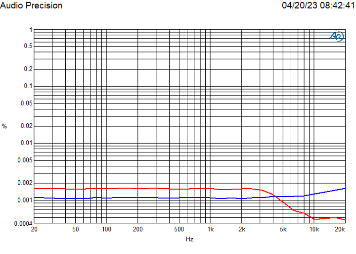
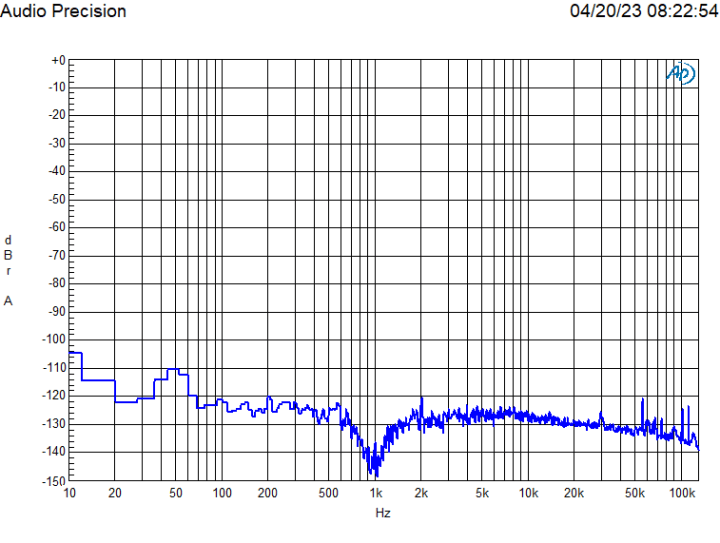
Plot B shows THD+N from 20 Hz to 20 kHz at input signal of 1 V and a bandwidth of 80 kHz. The blue plot is measured with P1 set to minimum. THD+N varies from 0.0011 % to 0.0016 % at 20 kHz. The red plot is measured with P1 set to maximum. Above 3 kHz THD +N decreases to 0.00048 % at 20 kHz. The relative noise level is lower due to the higher output level toward 20 kHz.
Plot C shows a FFT of 1 kHz at 1 V with P1 set to maximum. A 2nd harmonic and a few artifacts above 50 kHz are visible just above the noise floor. THD+N at a bandwidth of 22 kHz is 0.0012 %.
Bill of materials
Resistor
R1, R15 = 100 Ω, 1%, 250 mW
R2, R4, R5, R10, R12, R16, R18, R19, R24, R26 = 10 kΩ, 1 %, 250 mW
R3, R17 = 30 kΩ, 1 %, 600 mW
R6, R7, R11, R20, R21, R25, R29 = 4.7 kΩ, 1 %, 250 mW
R8, R22 = 820 Ω, 1 %, 600 mW
R9, R23 = 1.40 kΩ, 1 %, 250 mW
R13, R27 = 47 Ω, 1 %, 250 mW
R14, R28 = 100 kΩ, 1 %, 250 mW
P1 = 10 kΩ, 2 gangs potentiometer, lin., PC-16 series Piher (PC16DH-10IP06-103A2020-TA)
Capacitor
C1, C2, C3, C8, C9, C10 = 4.7 nF, 1%, 63 V, radial, polystyrene, 7.5x7.5 mm (RS Pro Extended Foil EXFS Series)
C4, C11 = 330 pF, 1 %, 630 V, body 12.9x5 mm axial, polystyrene (LCR Components FSCEX 330PF 1% 630V)
C5, C12 = 4.7 µF, 10 %, 50 V, pitch 5 mm (Wima MKS2B044701K00KSSD)
C6, C7, C13, C14 = 100 nF, 10 %, 50 V, ceramic X7R, pitch 5 mm
C15, C16 = 220 µF, 20 %, 35 V, pitch 3.5 mm, Diam. 8 mm (Rubycon 35ZLK220M8X16)
Semiconductor
D1, D2, D3, D4 = 1N4148, DO-35
LED1 = LED, green, 3 mm (T-1), 76° , 10 mcd
IC1, IC2, IC3, IC4 = LME49720NA/NOPB, DIP-8
Other
K1, K2, K3, K4 = 2x1 pin header, pitch 2.54 mm, vertical
K1, K2, K3, K4 = RCA audio connector, chassis mount (not on PCB)
K5 = 3way screw terminal block, pitch 5 mm (Phoenix Contact MKDSN 1,5/3-5,08)
IC1, IC2, IC3, IC4 = DIP-8 IC socket
Misc.
PCB 230190-1 v1.1
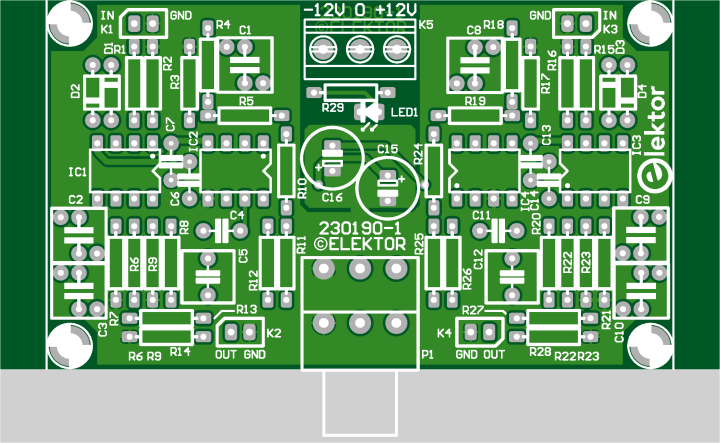
Schematic of the 2nd Order Adjustable Treble Boost (230190-1 v1.1)
The principle of the circuit is simple, sum the output of a 2nd order highpass filter and it’s input signal. Just adding the two signals will have an unwanted effect on the desired summation caused by the phase change of the filter. To correct this the input signal of filter IC1B is corrected by allpass filter IC2A before summation with its output signal, by summing amplifier IC2B, otherwise some frequencies can get attenuated. A second order critically damped filter has the same phase change as an allpass filter. However the slope of this type of filter is not as steep as desired. Using a Butterworth filter instead causes the phase change to be different and the allpass can’t quite correct this steeper filter. This results in a small variance of the gain at lower frequencies, less then +0.2 dB around 900 Hz and -0.3 dB around 3 kHz, depending on the exact operating point of the allpas filter. To make the highpass and allpass filter independent of the impedance of the source signal voltage follower IC1A is added at the input. D1, D2 and R1 protect the input of the opamp against possible overvoltage and spikes. Input impedance is mainly defined by R2, so 10 kΩ. The output signal of the allpass filter is directly connected to the summing amplifier. The gain is defined by the ratio of R12 and R10, so unity gain. The gain of output signal of the highpass filter is set by the ratio of R12 and R11.
To make it easier to change the frequency at which the treble boost starts, should anyone require a different correction, the Butterworth filter also has a small gain of 1,5857 x. At the theoretical gain of 3 - √2 (= 1.5858) the resistors and capacitors have the same values, so C2 = C3 and R6 = R7. If a change is needed the circuit is simple enough to simulate it as a way to find out what the change of component values has on the characteristic of the treble boost. Capacitor C1 has the same value as C2 and C3 and make it easy to change the operating point, all 3 capacitors should have the same value. Of course changing R3 and R6 and R7 proportionately is also an option. The value of 4.7 nF (C1/C2/C3) is chosen because it is available as 1 % polystyrene capacitor and this dielectric is an excellent choice to guarantee low tolerance and low distortion. Also the reason why C4 is a 1 % polystyrene capacitor (axial, placed upright). The low tolerance of all filter components make the phase change between the two chancels as low as possible. A cheaper solution but much lower quality and higher tolerance is the use of standard 5 mm PET capacitors for C1…C3/C8…C10 and 5 mm ceramic (use at least NP0/C0G dielectric) for C4 and C11.
To have a total gain of 12 dB (4x) around 17 kHz the gain of the highpass filter and the small attenuation caused by the bandwidth limiting capacitor C4 also have to be taken into account, in addition to the ratio of R12/R11. Total gain should be 3 to get 4 times the input signal at the output of the summing amplifier. Without C4 maximum gain of the highest frequencies would be 3,37: (1+820 Ω/1.4 kΩ)*(10 kΩ/4.7 kΩ).
Although a quad opamp could have been used for each channel, the amount of high quality dual opamps is far greater and some have much better properties. An excellent choice is the LME49720 which is also (still) available in an 8 pins DIP package. Its high Gain Bandwidth Product of 55 MHz and extreme low distortion of less than 0.00007 % at 20 kHz in a 2 kΩ load (3 VRMS , +/-12 V) make it an excellent choice for this type of circuit. It also has a very low input offset voltage. Offset at the output of the summing amplifiers varies slightly with the position of P1 but stayed below 1 mV in the prototype. Should another opamp be used the offset can be much higher. Capacitor C5 blocks any DC voltage at the output. The cutoff frequency with a 10 kΩ load is 3.7 Hz.
Total quiescent current of the prototype is +44.7/-42.6 mA. The current through LED1 is 2.1 mA. The quiescent current of a LME49720 is typically rated 10 mA at +/-15 V. To use a standard AC adapter as power supply a DC-DC converter is one way of creating a symmetrical power supply for the treble boost. Total power of the circuit is 1.05 W, so a 1 W DC-DC converter should probably be sufficient, but one with a slightly higher power output is advisable. Use one with regulated outputs. Most symmetrical DC-DC converter series have an output voltage of +/-12 V, the reason why +/-12 V is chosen as the power supply voltage. However, power supply voltage range of the LME49720 is +/-2.5 to +/-17 V.
The width of the PCB is extended to almost 100 mm so it can fit in the 1455 series of Hammond enclosures. The PCB can be shortened to the white lines. 4 mounting hole can be used to fasten the PCB in any other enclosure. Enclosure 1455N1201 would be a nice choice. However, the potentiometer is about 1 mm too high if the PCB is placed in the lowest slots. Bending the wider part of the leads of the potentiometer slightly towards the body can make the potentiometer low enough to make it fit. Just a thought. Another option is placing the potentiometer with its thread through the front (of any enclosure) and use short thin flexible wires to connect it to the PCB. This way any linear dual gang 10 kΩ potentiometer can be used.
Warning: as with all treble controls at high volume settings and maximum treble boost the power output of a power amplifier to a tweeter can be too much and damage it! An increase of 4 times in amplitude means 16 times an increase in power!
Measurements prototype
Vin max (1 kHz, THD = 0.1 %) 7.9 V
Quiescent current (Vs +/-12 V) +44.7/-42.6 mA
Bandwidth (P1 min.) 3.7 Hz…48 kHz (load 10 kΩ)
Max. Gain @ 17 kHz (P1 max.) 12 dB
THD+N (1 kHz, 1 V, P1 min.) 0.0008 % (B= 22 kHz)
THD+N (1 kHz, 1 V, P1 max.) 0.0012 % (B = 22 kHz)
THD+N (1 kHz, 1 V, P1 min.) 0.0012 % (B = 80 kHz)
THD+N (1 kHz, 1 V, P1 max.) 0.0016 % (B = 80 kHz)
Plot A shows the amplitude from 10 to 100 kHz and gives a good impression of the characteristic of this adjustable treble boost. P1 is adjusted to have 1 dB steps at 17 kHz. In the lowest but one plot P1 is adjusted to 0 dB gain at 17 KHz. For the lowest plot P1 is set to its minimum position. Depending on the setting of P1 the operating point shifts from approximately 6 kHz to 3 kHz when P1 is adjusted from minimum to maximum setting.
Plot B shows THD+N from 20 Hz to 20 kHz at input signal of 1 V and a bandwidth of 80 kHz. The blue plot is measured with P1 set to minimum. THD+N varies from 0.0011 % to 0.0016 % at 20 kHz. The red plot is measured with P1 set to maximum. Above 3 kHz THD +N decreases to 0.00048 % at 20 kHz. The relative noise level is lower due to the higher output level toward 20 kHz.
Plot C shows a FFT of 1 kHz at 1 V with P1 set to maximum. A 2nd harmonic and a few artifacts above 50 kHz are visible just above the noise floor. THD+N at a bandwidth of 22 kHz is 0.0012 %.
Bill of materials
Resistor
R1, R15 = 100 Ω, 1%, 250 mW
R2, R4, R5, R10, R12, R16, R18, R19, R24, R26 = 10 kΩ, 1 %, 250 mW
R3, R17 = 30 kΩ, 1 %, 600 mW
R6, R7, R11, R20, R21, R25, R29 = 4.7 kΩ, 1 %, 250 mW
R8, R22 = 820 Ω, 1 %, 600 mW
R9, R23 = 1.40 kΩ, 1 %, 250 mW
R13, R27 = 47 Ω, 1 %, 250 mW
R14, R28 = 100 kΩ, 1 %, 250 mW
P1 = 10 kΩ, 2 gangs potentiometer, lin., PC-16 series Piher (PC16DH-10IP06-103A2020-TA)
Capacitor
C1, C2, C3, C8, C9, C10 = 4.7 nF, 1%, 63 V, radial, polystyrene, 7.5x7.5 mm (RS Pro Extended Foil EXFS Series)
C4, C11 = 330 pF, 1 %, 630 V, body 12.9x5 mm axial, polystyrene (LCR Components FSCEX 330PF 1% 630V)
C5, C12 = 4.7 µF, 10 %, 50 V, pitch 5 mm (Wima MKS2B044701K00KSSD)
C6, C7, C13, C14 = 100 nF, 10 %, 50 V, ceramic X7R, pitch 5 mm
C15, C16 = 220 µF, 20 %, 35 V, pitch 3.5 mm, Diam. 8 mm (Rubycon 35ZLK220M8X16)
Semiconductor
D1, D2, D3, D4 = 1N4148, DO-35
LED1 = LED, green, 3 mm (T-1), 76° , 10 mcd
IC1, IC2, IC3, IC4 = LME49720NA/NOPB, DIP-8
Other
K1, K2, K3, K4 = 2x1 pin header, pitch 2.54 mm, vertical
K1, K2, K3, K4 = RCA audio connector, chassis mount (not on PCB)
K5 = 3way screw terminal block, pitch 5 mm (Phoenix Contact MKDSN 1,5/3-5,08)
IC1, IC2, IC3, IC4 = DIP-8 IC socket
Misc.
PCB 230190-1 v1.1
Top overlay of the PCB of the 2nd Order Adjustable trebel Boost (230190-1 v1.1)
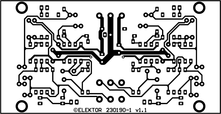
Copper on top of PCB of 2nd Order Adjustable Treble Boost
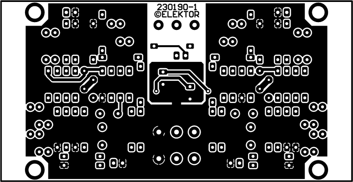
Copper on bottom of PCB of 2nd Order Adjustable Treble Boost
Copper on top of PCB of 2nd Order Adjustable Treble Boost
Copper on bottom of PCB of 2nd Order Adjustable Treble Boost
Diskussion (1 Kommentar)