
Driver for WS2812B Neopixel
Transmitting Data to WS2812B using a Timer and PWM
The W2812 Protocol
The transmission of data from a microcontroller (μC) to neopixel (WS2812B) requires a special serial protocol. It is a square wave signal with a variable duty cycle. The frequency of this signal is 800 kHz. 350 ns High level means '0' and 700 ns means '1' both with a tolerance of 150 ns. This is very similar to a PWM signal with variable duty cycle.
Transferring data to die Neopixel
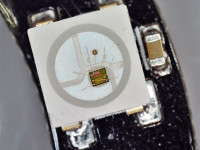
The transmission protocol is reminiscent of a PWM signal. Therefore, it is certainly a clever idea to use a PWM to generate it. The driver is written for an ATMEGA 48/88/168 with 20 MHz clock frequency but can also be adapted to other types. The Din input of the last neopixel is connected to OC0B (PIN11) of the AVR. For testing, a circular module is used on which 12 neopixels are arranged.
Timer 0 of the ATMEGA is used to transmit the data to the neopixel via PWM. The timer is configured in mode 7. This is a fast PWM mode that makes it possible to choose the resolution. The maximum number of clocks is stored in OCR0A. This value can be calculated by dividing the clock frequency of the ATMEGA by the frequency of the WS28125 protocol. So you get the value of 24 for OCR0A
The timer has been configured to set the output OC0B to Low for Compare Match B. When this happens is determined by the content of the OCR0B register. For the transmission of a logical 1, a Thigh of 650 μs was chosen. For a logical 0, Thigh was set at 400 μs. These values correspond to the specifications of the data sheet for WS2812B.
This results in the values for OCR0B, 12 counts for High and 7 counts for Low
If the counter reading reaches the maximum value (24), a timer overrun takes place, which triggers an interrupt. The associated ISR determines the next value for OCR0B depending on whether the bit being checked is a 1 or a 0. At the same time, the OCR0B register is updated with the current value at counter reading 0. In this way, all bytes are transferred to the neopixels. The time for the ISR is limited to a maximum of 1.25 μs. Therefore, high-level languages such as C or Bascom are not suitable for the ISR. The programs would take too long to run. The complete driver and also the ISR was programmed in assembler. Only in this way can the program duration remain within the limit of 1.25 μs.
Example program LED Control V1.1
LED Control V1.1 controls a ring of 12 neopixels. A group of three LEDs (green, red, blue) performs counter clockwise rotation. The program is written partly in Bascom and partly in assembler. The Bascom part contains all non-time-critical components, the assembler part the complete driver and thus the time-critical components.
LED Controll uses 4 variables. LED_data is an array of 39 bytes. The data for the green, red and blue are stored here for each neopixel. In addition, there are 3 bytes for a buffer, which is needed when moving the data. In Num_Bytes, the number of bytes in the array is stored without the bytes of the buffer. Mask contains the start value of the mask that is required for the test of bits in the driver. All these variables are required in the driver. Datapointer is used for operations with the LED_data array. The variable Num_Bytes is assigned the value 36 and Mask the binary value 10000000b.
Now constants are set that are needed to configure Timer 0. THigh and TLow contain the values for the Compare register OCR0B. TCCR0A_Con is required to configure the timer. Here it is specified that the output OCR0B is set to Low at Compare Match ( COM0B1=1, COM0B0=0 ) and the timer is operated in mode 7 ( WGM01=1, WGM00=1 + WGM02=1 ). In this mode, the resolution of the PWM can be selected. The maximum value is stored in OCR0A. There are two samples for the second configuration register TCCR0B. They are used to start and stop the counter. Timer 0 receives a basic configuration in the stopped state. PIN 11 (PD5) is configured as output OC0B and an ISR is assigned to the overflow interrupt.
The main program only ensures the rotation of the data in the array LED_data. After each run, the subroutine WS2812_send is called.
Subroutine WS2812_send
Used AVR register
R0 Register for testing LED data
R1 Register with the selection mask for
choosing a bit of LED data
R2 Register with LED data
R21 Number of bytes to transmit
R16 Register with PWM value for 0
R17 Register with PWM value for 1
R18 Register with the value of 1
R19 Control register
R20 Operation register
R22 Mask register bit check
After storing all required registers in the stack, the registers R16-R20 and the Output Compare register OCR0B are loaded with start parameters.
Then the index register X receives the address of the variable Mask. This is loaded into R1 and R22. With the variable Num_Bytes, the program proceeds in the same way and loads it into register R21.
Next, X is loaded with the address of the first data byte of Array LED_data and the content is loaded to R2. A check of bit 7 in R2 follows. The result , 1 or 0, determines which value is loaded into the Output Compare register. R1, the register with the selection mask, is shifted 1 bit to the right. After starting the timer 0, the program waits in a loop until the next overflow interrupt is triggered and the associated ISR is called or all bytes of array LED_Data have been transferred and an end id is set in R20 (R20=0x80). This terminates the loop, restores all used registers, and terminates the program.
The ISR Transmit
With each overflow interrupt, this program is called to determine whether the next bit is a 1 or 0. Accordingly, the constants THigh or TLow are loaded into the Capture Compare register OCR0B. At the beginning, the mask register is tested to see if it contains a 0. This would mean that the current byte has been transferred complete. If this is not the case -> ISR_Transmit_1.
The number of bytes to be sent is incremented and checks whether all bytes have been transferred (R21=0) which leads to the end of the program (-> ISR_ENDE). Timer 0 is stopped, and the end ID is set (R20=0x80).
If there are still bytes to send, the program loads the new byte and sets the mask for the bitwise test to the starting value (10000000b).
ISR_Transmit_1
Test register R0 is loaded with the current byte, and linked to the test mask in R1 . If R0 and R1 are identical, the tested bit was 1 -> ISR_Transmit_2
Other, the Capture Compare Register OCR0B is loaded with the contents of R16 (Tlow), the test mask shifted one bit to the right and the program exits.
ISR_Transmit_2
After the value for a 1 has been loaded into the Capture Compare register OCR0B and the test mask has been moved one bit to the right, the program ends.
In the ISR, if possible, only register commands are used. The reason is that the ISR cannot be longer than 24 clock cycles and these commands only need one clock cycle to execute. Therefore, all required variables are stored in registers.
The transmission of data from a microcontroller (μC) to neopixel (WS2812B) requires a special serial protocol. It is a square wave signal with a variable duty cycle. The frequency of this signal is 800 kHz. 350 ns High level means '0' and 700 ns means '1' both with a tolerance of 150 ns. This is very similar to a PWM signal with variable duty cycle.
Transferring data to die Neopixel
The transmission protocol is reminiscent of a PWM signal. Therefore, it is certainly a clever idea to use a PWM to generate it. The driver is written for an ATMEGA 48/88/168 with 20 MHz clock frequency but can also be adapted to other types. The Din input of the last neopixel is connected to OC0B (PIN11) of the AVR. For testing, a circular module is used on which 12 neopixels are arranged.
Timer 0 of the ATMEGA is used to transmit the data to the neopixel via PWM. The timer is configured in mode 7. This is a fast PWM mode that makes it possible to choose the resolution. The maximum number of clocks is stored in OCR0A. This value can be calculated by dividing the clock frequency of the ATMEGA by the frequency of the WS28125 protocol. So you get the value of 24 for OCR0A
The timer has been configured to set the output OC0B to Low for Compare Match B. When this happens is determined by the content of the OCR0B register. For the transmission of a logical 1, a Thigh of 650 μs was chosen. For a logical 0, Thigh was set at 400 μs. These values correspond to the specifications of the data sheet for WS2812B.
This results in the values for OCR0B, 12 counts for High and 7 counts for Low
If the counter reading reaches the maximum value (24), a timer overrun takes place, which triggers an interrupt. The associated ISR determines the next value for OCR0B depending on whether the bit being checked is a 1 or a 0. At the same time, the OCR0B register is updated with the current value at counter reading 0. In this way, all bytes are transferred to the neopixels. The time for the ISR is limited to a maximum of 1.25 μs. Therefore, high-level languages such as C or Bascom are not suitable for the ISR. The programs would take too long to run. The complete driver and also the ISR was programmed in assembler. Only in this way can the program duration remain within the limit of 1.25 μs.
Example program LED Control V1.1
LED Control V1.1 controls a ring of 12 neopixels. A group of three LEDs (green, red, blue) performs counter clockwise rotation. The program is written partly in Bascom and partly in assembler. The Bascom part contains all non-time-critical components, the assembler part the complete driver and thus the time-critical components.
LED Controll uses 4 variables. LED_data is an array of 39 bytes. The data for the green, red and blue are stored here for each neopixel. In addition, there are 3 bytes for a buffer, which is needed when moving the data. In Num_Bytes, the number of bytes in the array is stored without the bytes of the buffer. Mask contains the start value of the mask that is required for the test of bits in the driver. All these variables are required in the driver. Datapointer is used for operations with the LED_data array. The variable Num_Bytes is assigned the value 36 and Mask the binary value 10000000b.
Now constants are set that are needed to configure Timer 0. THigh and TLow contain the values for the Compare register OCR0B. TCCR0A_Con is required to configure the timer. Here it is specified that the output OCR0B is set to Low at Compare Match ( COM0B1=1, COM0B0=0 ) and the timer is operated in mode 7 ( WGM01=1, WGM00=1 + WGM02=1 ). In this mode, the resolution of the PWM can be selected. The maximum value is stored in OCR0A. There are two samples for the second configuration register TCCR0B. They are used to start and stop the counter. Timer 0 receives a basic configuration in the stopped state. PIN 11 (PD5) is configured as output OC0B and an ISR is assigned to the overflow interrupt.
The main program only ensures the rotation of the data in the array LED_data. After each run, the subroutine WS2812_send is called.
Subroutine WS2812_send
Used AVR register
R0 Register for testing LED data
R1 Register with the selection mask for
choosing a bit of LED data
R2 Register with LED data
R21 Number of bytes to transmit
R16 Register with PWM value for 0
R17 Register with PWM value for 1
R18 Register with the value of 1
R19 Control register
R20 Operation register
R22 Mask register bit check
After storing all required registers in the stack, the registers R16-R20 and the Output Compare register OCR0B are loaded with start parameters.
Then the index register X receives the address of the variable Mask. This is loaded into R1 and R22. With the variable Num_Bytes, the program proceeds in the same way and loads it into register R21.
Next, X is loaded with the address of the first data byte of Array LED_data and the content is loaded to R2. A check of bit 7 in R2 follows. The result , 1 or 0, determines which value is loaded into the Output Compare register. R1, the register with the selection mask, is shifted 1 bit to the right. After starting the timer 0, the program waits in a loop until the next overflow interrupt is triggered and the associated ISR is called or all bytes of array LED_Data have been transferred and an end id is set in R20 (R20=0x80). This terminates the loop, restores all used registers, and terminates the program.
The ISR Transmit
With each overflow interrupt, this program is called to determine whether the next bit is a 1 or 0. Accordingly, the constants THigh or TLow are loaded into the Capture Compare register OCR0B. At the beginning, the mask register is tested to see if it contains a 0. This would mean that the current byte has been transferred complete. If this is not the case -> ISR_Transmit_1.
The number of bytes to be sent is incremented and checks whether all bytes have been transferred (R21=0) which leads to the end of the program (-> ISR_ENDE). Timer 0 is stopped, and the end ID is set (R20=0x80).
If there are still bytes to send, the program loads the new byte and sets the mask for the bitwise test to the starting value (10000000b).
ISR_Transmit_1
Test register R0 is loaded with the current byte, and linked to the test mask in R1 . If R0 and R1 are identical, the tested bit was 1 -> ISR_Transmit_2
Other, the Capture Compare Register OCR0B is loaded with the contents of R16 (Tlow), the test mask shifted one bit to the right and the program exits.
ISR_Transmit_2
After the value for a 1 has been loaded into the Capture Compare register OCR0B and the test mask has been moved one bit to the right, the program ends.
In the ISR, if possible, only register commands are used. The reason is that the ISR cannot be longer than 24 clock cycles and these commands only need one clock cycle to execute. Therefore, all required variables are stored in registers.
Diskussion (2 Kommentare)